

Stacked body-contacted field effect transistor
a field effect transistor and body contact technology, applied in the field of stacking body contact field effect transistors, can solve the problems of increasing integration of wireless communication devices, complex, and low power consumption, and achieve the effects of reducing the off-state drain-to-source capacitance of the fet, saving space, and saving spa
- Summary
- Abstract
- Description
- Claims
- Application Information
AI Technical Summary
Benefits of technology
Problems solved by technology
Method used
Image

Examples
Embodiment Construction
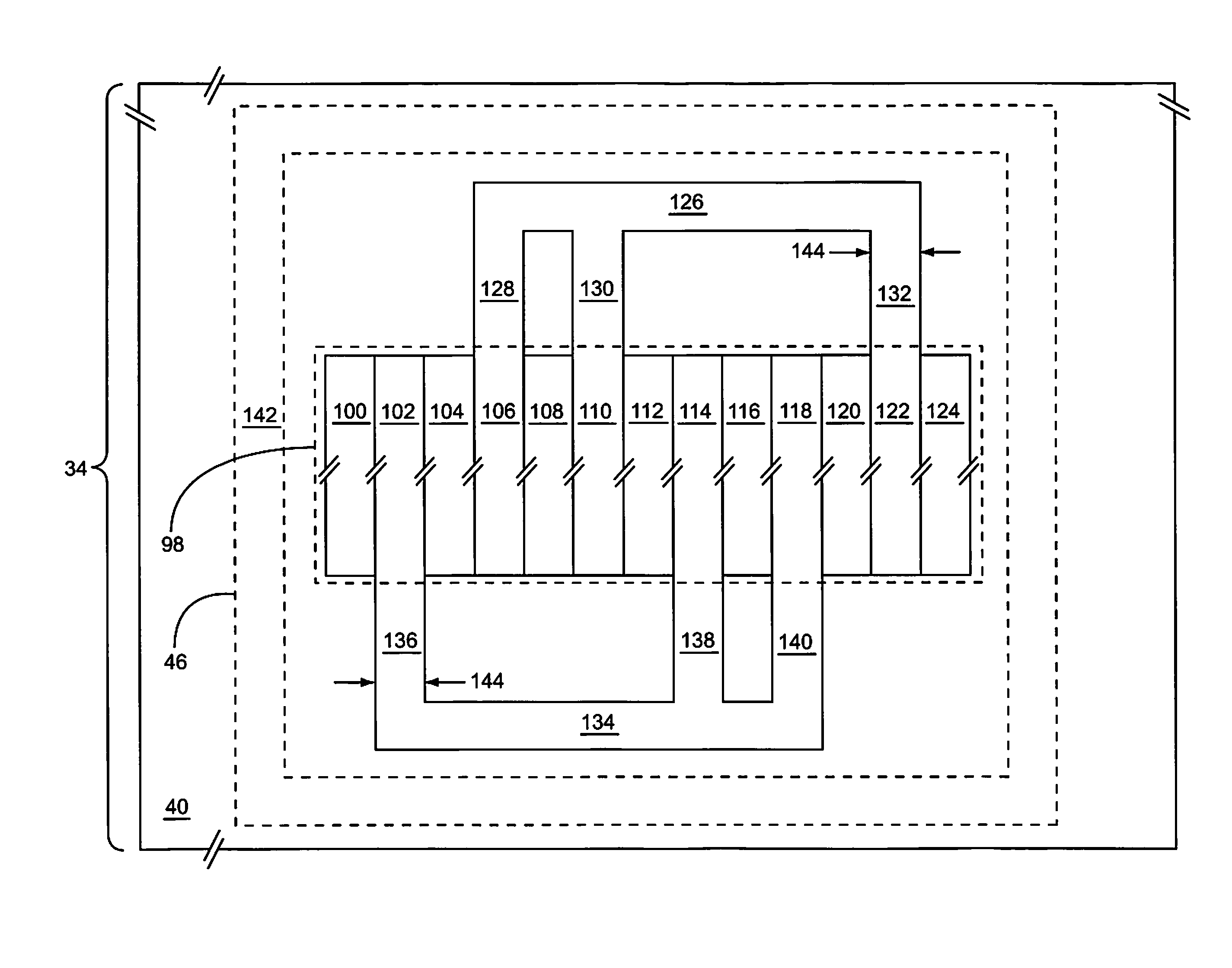
[0005]The present disclosure relates to a stacked body-contacted field effect transistor (FET) that includes multiple body-contacted FETs coupled in series and a lateral isolation band encircling a periphery of the multiple FETs. The multiple FETs include a first end FET having a first body, which is not directly connected to any body of any other of the multiple FETs, and a second end FET having a second body, which is not directly connected to any body of any other of the multiple FETs. The multiple FETs may include inner FETs that incorporate merged source-drains to save space. By keeping the bodies electrically separated from one another, the full benefits of body-contacting may be realized. However, incorporating multiple FETs within a single lateral isolation band further saves space. Each of the multiple FETs is body-contacted and may receive reverse body biasing when the FET is in an OFF state, thereby reducing an OFF state drain-to-source capacitance of the FET.
[0006]Those ...
PUM
 Abstract
Description
Claims
Application Information