Latch circuit with a bridging device

a latch circuit and bridging device technology, applied in the direction of pulse generators, pulse techniques, electrical apparatus, etc., can solve the problems of large power consumption in the clock network, significant power dissipation, and limited performance of integrated circuit devices, so as to reduce clock energy, reduce load, and improve latch circuit operation.

Active Publication Date: 2014-02-25
NVIDIA CORP
View PDF9 Cites 5 Cited by
  • Summary
  • Abstract
  • Description
  • Claims
  • Application Information

AI Technical Summary

Benefits of technology

[0012]One advantage of the disclosed latch circuit is that the transistor device load on the clock signal is reduced to only two or three transistor gates. Therefore, the clock energy is reduced significantly compared with latch circuit having greater loads on the clock signal. Versions of the latch circuit with the bridging transistor activated by a clock (or enable signal) are also completely static and do not rely on sizing relationships between the different transistors. Versions of the latch circuit that use a weak always-on bridging device present only two loads to the clock (or enable signal). The latch circuit operations are robust, even when the characteristics of the transistors vary due to the fabrication process.

Problems solved by technology

Power dissipation is a significant problem in conventional integrated circuits.
In many applications, the performance of integrated circuit devices is limited by the amount of energy consumed by the circuitry implementing a function rather than by the die area of the circuitry.
A large fraction of the power dissipated in conventional digital integrated circuits is consumed in the clock network.
The weak devices are slow and do have a negative impact on the speed of the latch circuit 250.
These conflicting demands are difficult to balance, particularly as the fabrication process varies.

Method used


Image

  • Latch circuit with a bridging device
  • Latch circuit with a bridging device
  • Latch circuit with a bridging device

Examples


Embodiment Construction

[0027]In the following description, numerous specific details are set forth to provide a more thorough understanding of the present invention. However, it will be apparent to one of skill in the art that the present invention may be practiced without one or more of these specific details. In other instances, well-known features have not been described in order to avoid obscuring the present invention.

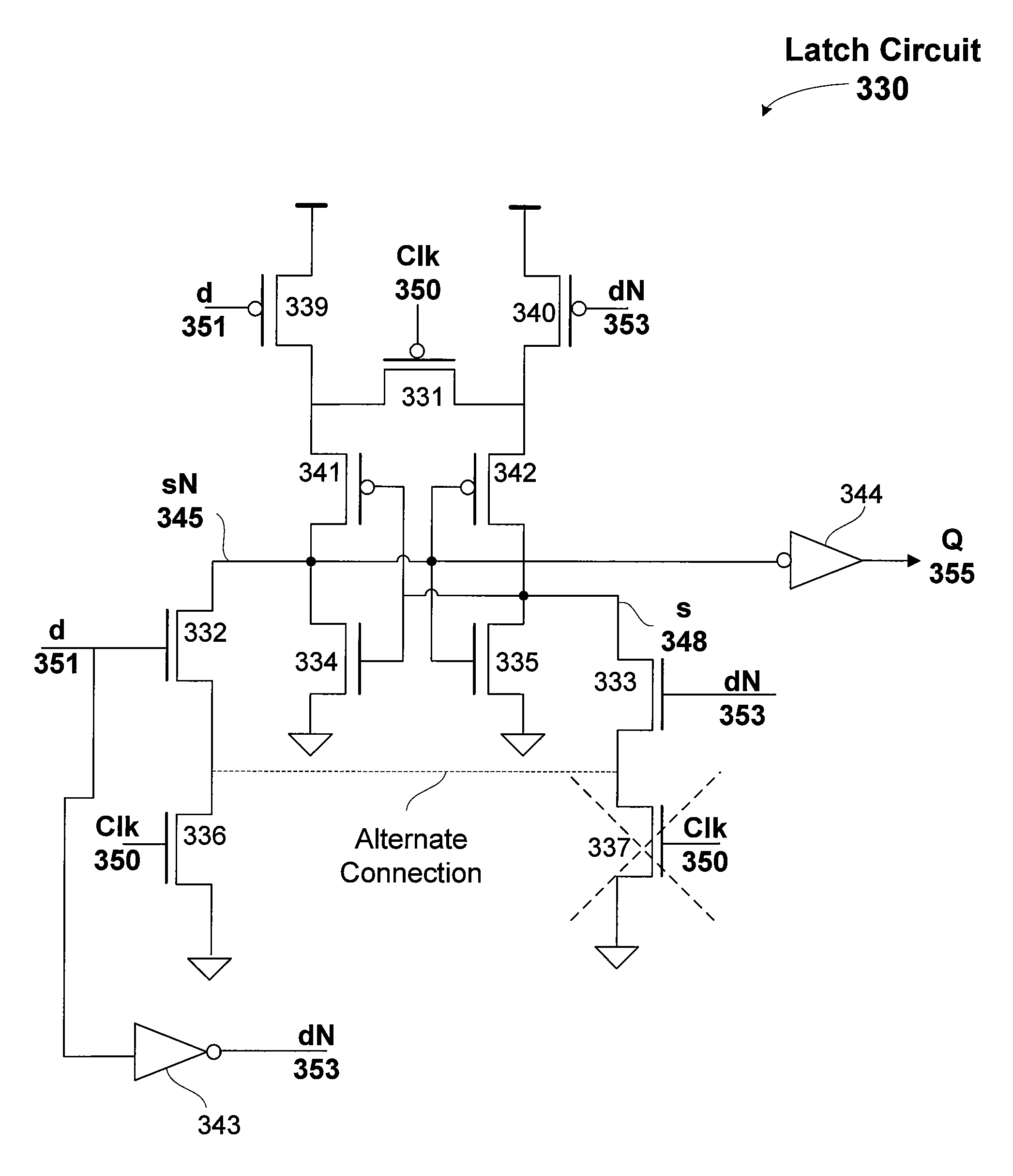
[0028]FIG. 3A illustrates a low-clock-energy latch circuit 300 that is transparent when the clock signal, Clk 320 is low, according to one embodiment of the invention. The latch circuit 300 is a fully-static, clock-energy-efficient latch that presents only three loads to the clock and which does not depend on transistor device size ratios. With only three minimum sized clock loads, the latch circuit 300 should consume only a third of the clock energy that is consumed by a conventional pass-gate latch (dependent on transistor sizing). The total number of transistors included in the latch...


PUM


Abstract

One embodiment of the present invention sets forth a technique for capturing and holding a level of an input signal using a latch circuit that presents a low number of loads to the clock signal. The clock is only coupled to a bridging transistor and a pair of clock-activated pull-down or pull-up transistors. The level of the input signal is propagated to the output signal when the storage sub-circuit is not enabled. The storage sub-circuit is enabled by the bridging transistor and a propagation sub-circuit is activated and deactivated by the pair of clock-activated transistors.

Description

BACKGROUND OF THE INVENTION[0001]1. Field of the Invention[0002]The present invention generally relates to digital latch circuits and more specifically to a low-clock-energy latch circuit.[0003]2. Description of the Related Art[0004]Power dissipation is a significant problem in conventional integrated circuits. In many applications, the performance of integrated circuit devices is limited by the amount of energy consumed by the circuitry implementing a function rather than by the die area of the circuitry. A large fraction of the power dissipated in conventional digital integrated circuits is consumed in the clock network. The amount of energy that is consumed by flip-flops due to data transitions is small because the activity factor, the fraction of time the data input of the flip-flop toggles, is quite low, typically about 5-10%. In contrast, the clock input load and clock energy is a particularly important metric for determining the energy that is consumed by the latches and flip...

Claims


Application Information

Patent Timeline
Patent Type & Authority Patents(United States)
IPC IPC(8): H03K3/356
CPCH03K3/356191H03K3/356026H03K3/356H03K3/356147H03K3/356052
Inventor ELKIN, ILYASDALLY, WILLIAM JAMESALBEN, JONAH M.
Owner NVIDIA CORP
Why Eureka
Try Eureka