

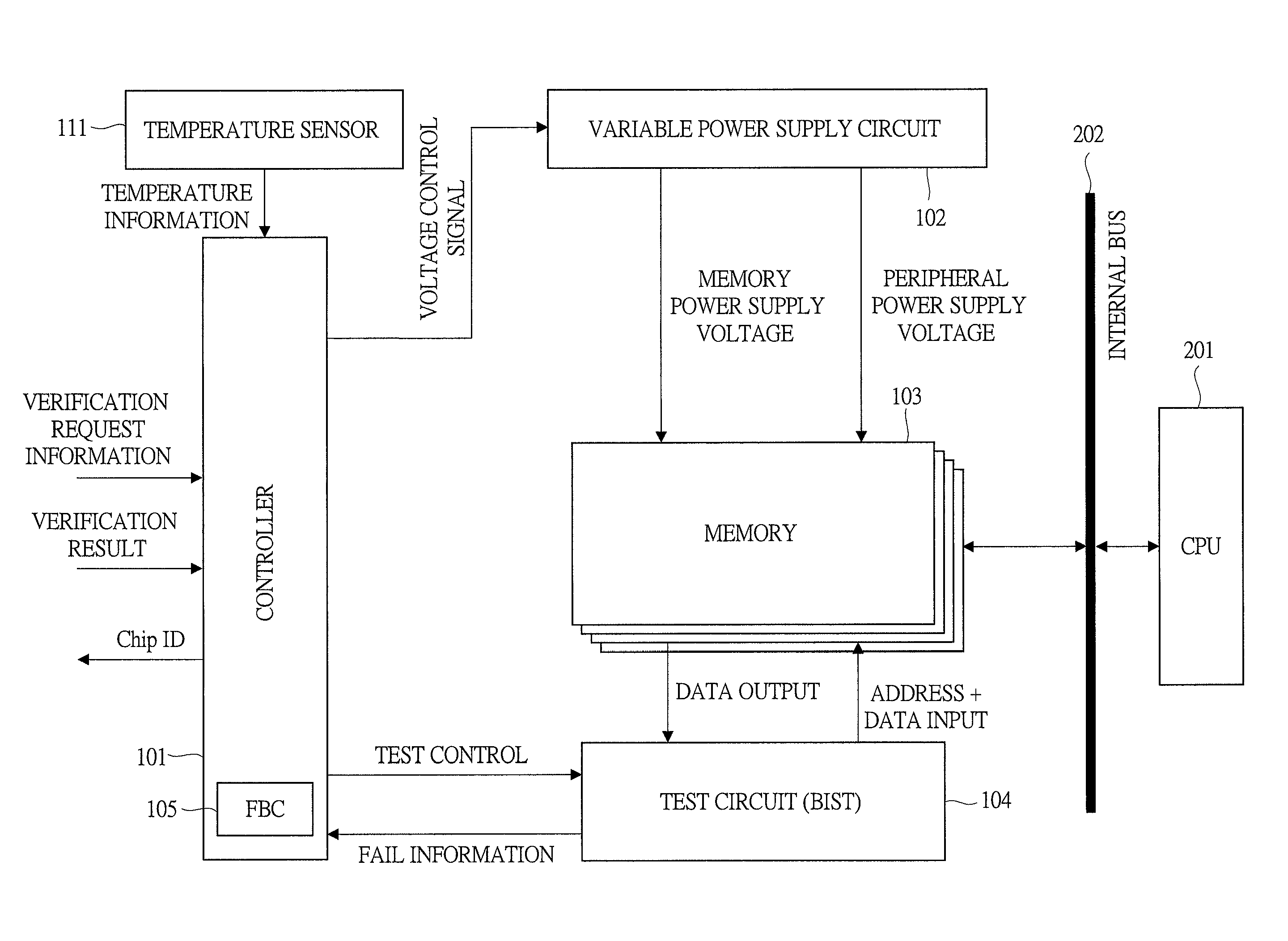
Semiconductor device
a semiconductor and device technology, applied in the field of semiconductor device verification, can solve the problems of increased cost, falsification of data written at the manufacturing, increased cost, etc., and achieve the effect of increasing cos
- Summary
- Abstract
- Description
- Claims
- Application Information
AI Technical Summary
Benefits of technology
Problems solved by technology
Method used
Image

Examples
first embodiment
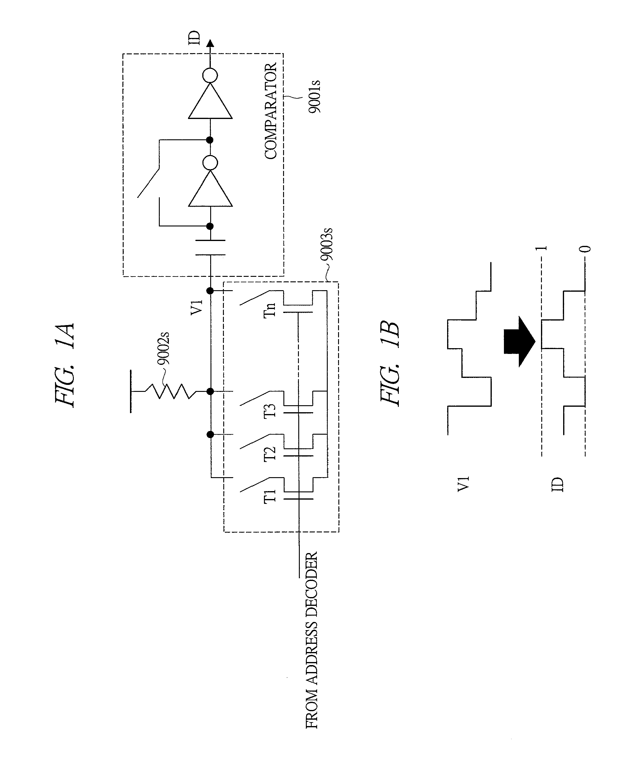
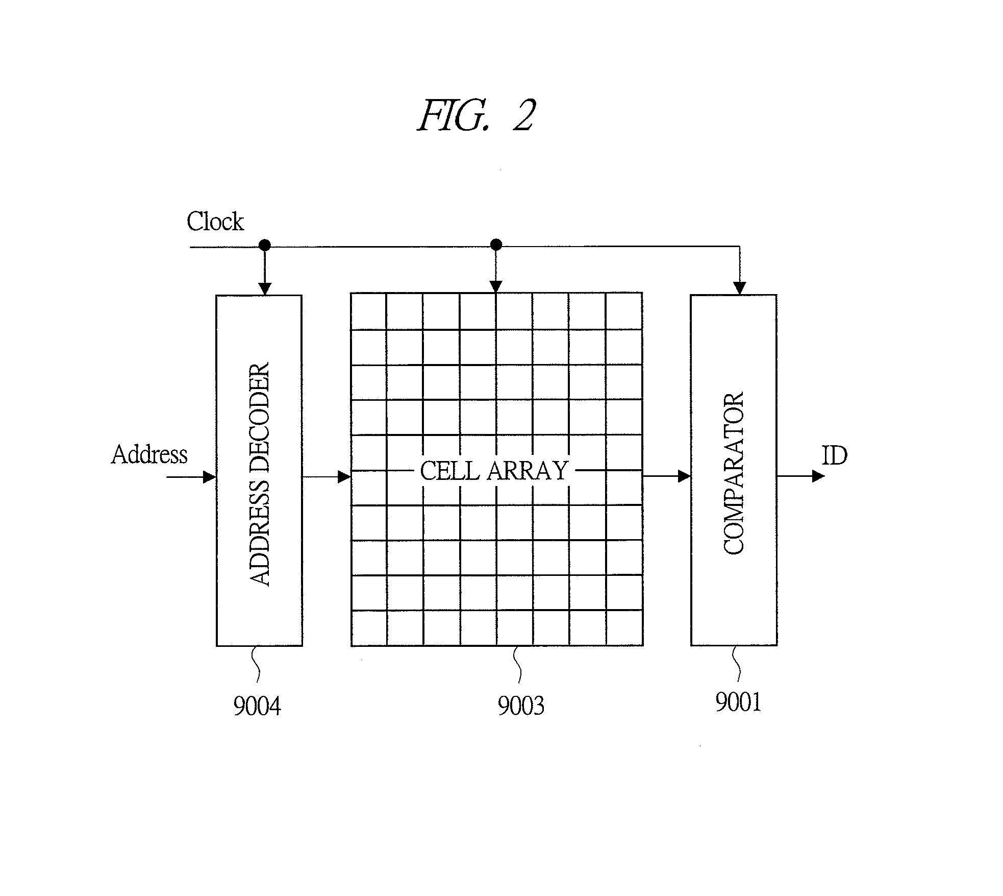
[0056]FIG. 4 is a conceptual diagram showing a basic concept of an operation according to a first embodiment of the present invention. And, FIG. 5 is a diagram showing an example in generating a chip-unique ID according to the first embodiment of the present invention.
[0057]In the present invention, a fact that an error is caused by gradually decreasing an operation voltage of a transistor in a chip is used for generating the chip-unique ID. Note that a dynamic chip such as a DRAM is assumed here.
[0058]As clearly seen from FIG. 4, as long as a non-defective product, all transistors perform a normal operation when a standard voltage is applied to the transistors in a chip. Note that the standard voltage is a power supply voltage used for the normal operation, and the normal operation is a state in which a power supply voltage used for memory reading / updating operation is applied as assumed in a case that a non-defective information storage medium such as a non-defective DRAM is mount...
second embodiment
[0124]Next, a second embodiment of the present invention is described with reference to figures.
[0125]The first embodiment of the present invention describes the basic operation of the present invention. However, in the acquisition of the fail bit map which is easily executed by the description of the flowchart, there is a high possibility that a reproducibility problem arises in, more particularly, the SRAM. Accordingly, improvement of the reproducibility of the fail bit map is described.
[0126]Further, in the present embodiment, improvement of reproducibility of the fail bit map by adjusting an assist level of the SRAM is discussed.
[0127]FIG. 10 is a circuit diagram showing the SRAM and voltages targeted for adjusting the assist level according to the second embodiment of the present invention.
[0128]First, the basic structure of the SRAM is described.
[0129]To this SRAM, three voltages are supplied. That is, they are a word-line potential Vwl, a bit-line potential Vbl, and a memory-...
third embodiment
[0148]Next, a third embodiment of the present invention is described.
[0149]In the first embodiment, as seen from FIG. 8, every time the verification request is issued, the memory BIST is operated to acquire the fail bit map.
[0150]By contrast, the present embodiment has a feature of using the data retained in the memory cell at power-on time as the chip-unique ID.
[0151]The data retained in the memory cell at the power-on time is determined by the random variation of the transistors of the memory cell. This value is retained in an arbitrary location in the memory, and is outputted when the verification request is issued, so that the reproducibility of the acquired data is improved. This is because it is not required to change the power supply voltage as different from the steps S1101 and S1105 (see FIG. 8).
[0152]However, the following points should be noted.
[0153]When the memory-line potential Vmc and the word-line potential Vwl (see FIG. 10) are simultaneously applied, there is a pos...
PUM
 Abstract
Description
Claims
Application Information