Electronic component

a technology of electronic components and components, applied in the field of electronic components, can solve the problems of reducing the functionality of electronic components, reducing reducing the selection of suitable film materials, etc., and achieves the effects of reducing the functionality of electronic components, reducing the tendency to oxide formation, and good electrical conductivity

Inactive Publication Date: 2014-04-15
ROBERT BOSCH GMBH
View PDF18 Cites 0 Cited by
  • Summary
  • Abstract
  • Description
  • Claims
  • Application Information

AI Technical Summary

Benefits of technology

[0012]The risk of the thin films tearing off at steps or edges is increased due to the fact that necessary semiconductor processes do not allow isotropic deposition of the thin films. In addition, coordination of multiple processes with one another is not possible without a certain degree of imprecision. The imprecision results, for example, from the resolution of the lithography during manufacture. This prevents exact adjustment of multiple layers to one another.
[0013]However, by using the electronic component according to the present invention, in which the printed conductor structure has a region which is covered by the film for the purpose of contacting, such tearing off is avoided due to the fact that not just vertical regions are connected to one another; rather, horizontal regions are also connected via the covering. The contacting thus remains, even in the case of different thermal expansions of the materials of the various layers.
[0015]To achieve stable contacting and to avoid tearing off due to different thermal expansions, for example, in another specific embodiment the region which is covered by the film has a smaller layer thickness than the film. The covered region preferably has a height in the range of 1 nm to 200 nm. As a result of the layer thickness of the covered region being smaller than that of the film which covers the region, the situation is avoided that a step which corresponds at least to the thickness of the film must be overcome when the film is applied. Thus, a continuous film which overcomes the step at the end of the covered region may be provided when it is applied. The risk of tearing due to different thermal expansions, for example, is thus avoided.
[0019]The material of the film, which has a smaller layer thickness than the printed conductor structure, is also preferably selected from the group composed of titanium, platinum, gold, aluminum, copper, chromium, nickel, and tantalum, compounds of these elements with oxygen, nitrogen, carbon, and silicon, and alloys of these elements. The advantage of using these elements is that they have good electrical conductivity. In addition, the tendency toward oxide formation is low, or may be minimized by providing an oxide layer on the surface. The situation is thus avoided that the material of the printed conductor structure or of the film experiences a loss in conductivity due to oxidation, and as a result the functionality of the electronic component is reduced or even completely lost.

Problems solved by technology

In the electronic components known from the related art, such tearing results, for example, due to the fact that different thermal expansions occur at high temperatures, which are necessary for gas sensors, for example, and which generally range from 25° C. to 800° C. In addition, with increasing operating temperature, for example, the selection of a suitable film material is more problematic.
This results in tearing off of the thin films primarily at steps.
However, such nonplanar transitions are unavoidable for many high-temperature semiconductor structures.

Method used


Image

  • Electronic component
  • Electronic component

Examples


Embodiment Construction

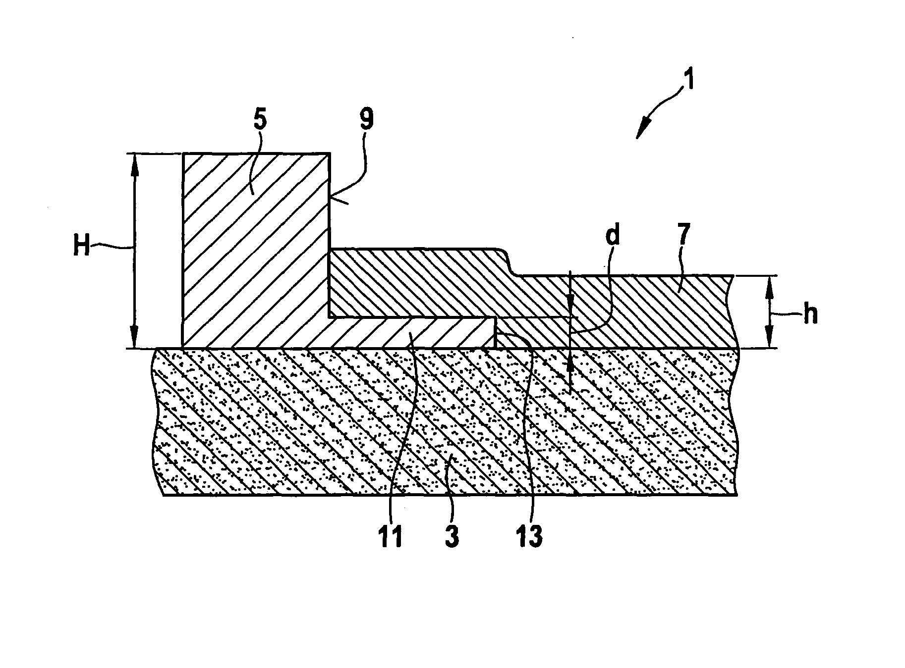
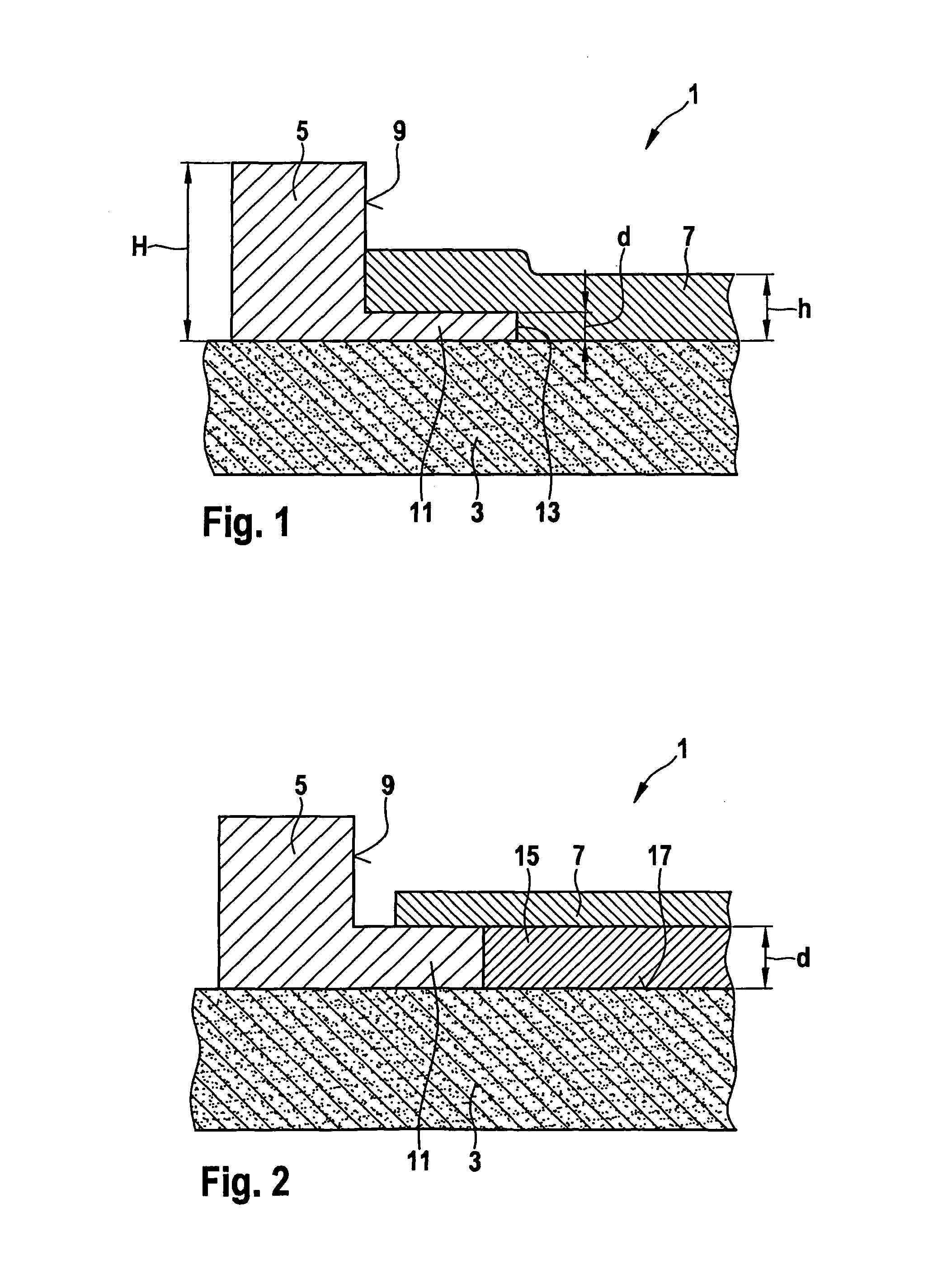
[0023]FIG. 1 illustrates a cross section of a detail of an electronic component. An electronic component 1 includes a substrate 3 to which a printed conductor structure 5 is applied.

[0024]Substrate 3 may be made of any desired material known to those skilled in the art. Substrate 3 is usually made of an electrically insulating material or a semiconductor material, for example. The selection of the material for substrate 3 depends on the intended use of the electronic component. Electrically insulating materials of which substrate 3 may be made are sapphire or SiO2, for example.

[0025]If the electronic component is to be used as a gas-sensitive field effect transistor, for example, substrate 3 is preferably made of a semiconductor material. Typically used semiconductor materials are, for example, semiconductor materials having a band gap greater than 2 eV. Of these, GaN and SiC are particularly preferred.

[0026]Printed conductor structure 5 is usually made of a material having good ele...


PUM


Abstract

An electronic component includes a printed conductor structure on a substrate, as well as a film which contacts the printed conductor structure. The film has a smaller layer thickness than the printed conductor. The printed conductor structure has a region which is covered by the film for the purpose of contacting.

Description

BACKGROUND OF THE INVENTION[0001]1. Field of the Invention[0002]The present invention relates to an electronic component having a printed conductor structure on a substrate.[0003]2. Description of Related Art[0004]Electronic components generally include a printed conductor structure on a substrate. Such electronic components may also have a thin film which contacts the printed conductor structure. The film generally has a smaller layer thickness than the printed conductor structure. Such electronic components are used, for example, as semiconductor-based gas-sensitive field effect transistors in sensor system applications. The film, which has a smaller layer thickness than the printed conductor structure, usually represents the gate electrode. Action by a gas to be detected generally results in a change in the current flowing through the transistor from the source electrode to the drain electrode.[0005]To allow gas detection with the aid of semiconductors, surfaces are necessary whi...

Claims


Application Information

Patent Timeline
Patent Type & Authority Patents(United States)
IPC IPC(8): H01L23/528
CPCG01N27/414
Inventor FIX, RICHARDSCHREY, FREDERIKWOLST, OLIVERDAUMILLER, INGOMARTIN, ALEXANDERLE-HUU, MARTINKUNZE, MIKE
Owner ROBERT BOSCH GMBH
Why Eureka
Try Eureka