

Solid-state imaging device with a photoelectric conversion element, and method thereof
a technology of photoelectric conversion element and solid-state imaging device, which is applied in the direction of radiological control device, television system scanning details, television system, etc., can solve the problem of accumulating dark current even during charge storag
- Summary
- Abstract
- Description
- Claims
- Application Information
AI Technical Summary
Benefits of technology
Problems solved by technology
Method used
Image

Examples
first embodiment
[0057]A solid-state imaging device according to a first embodiment of the present invention will be described.
[2-1 Structure and Fabrication Method]
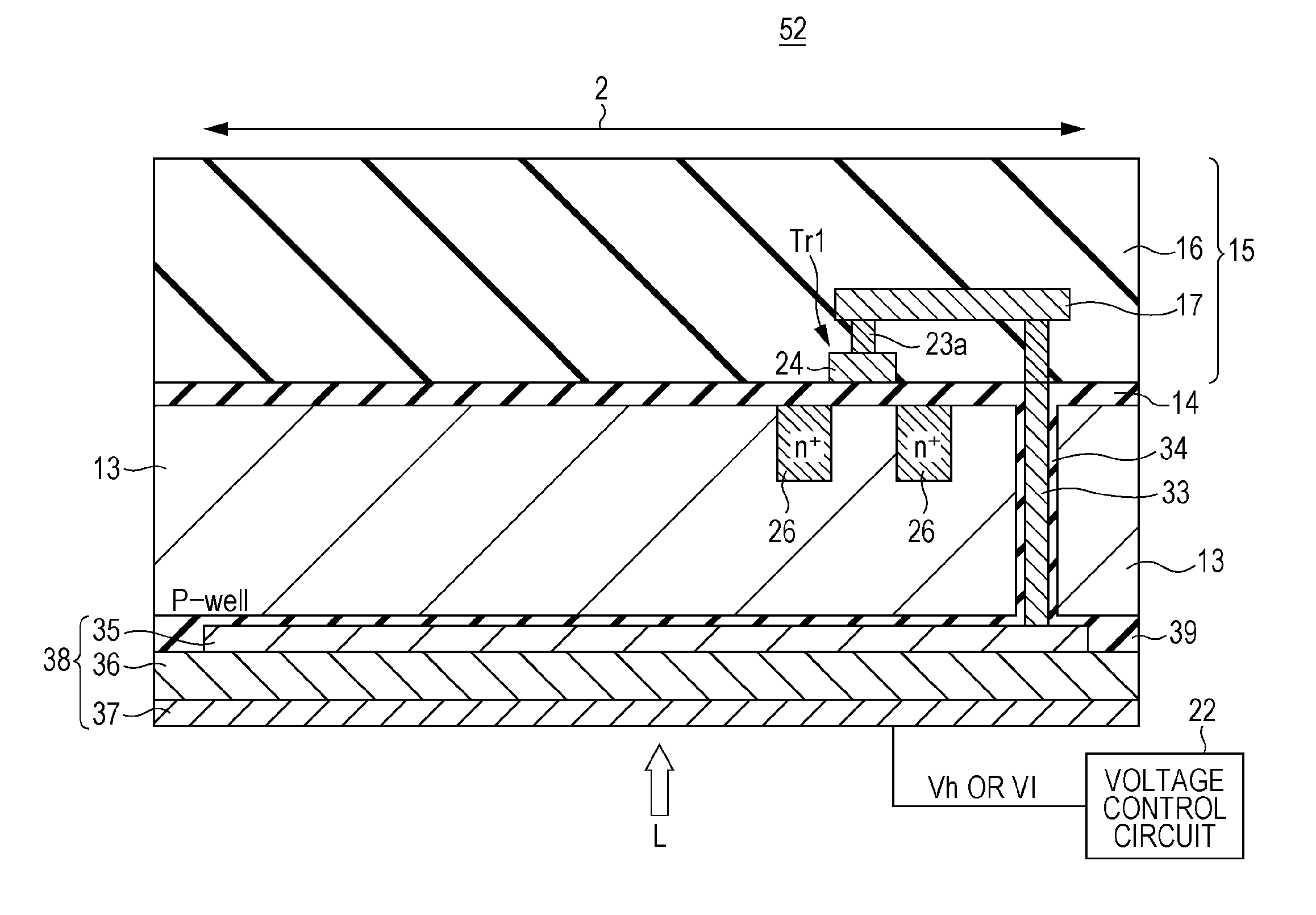
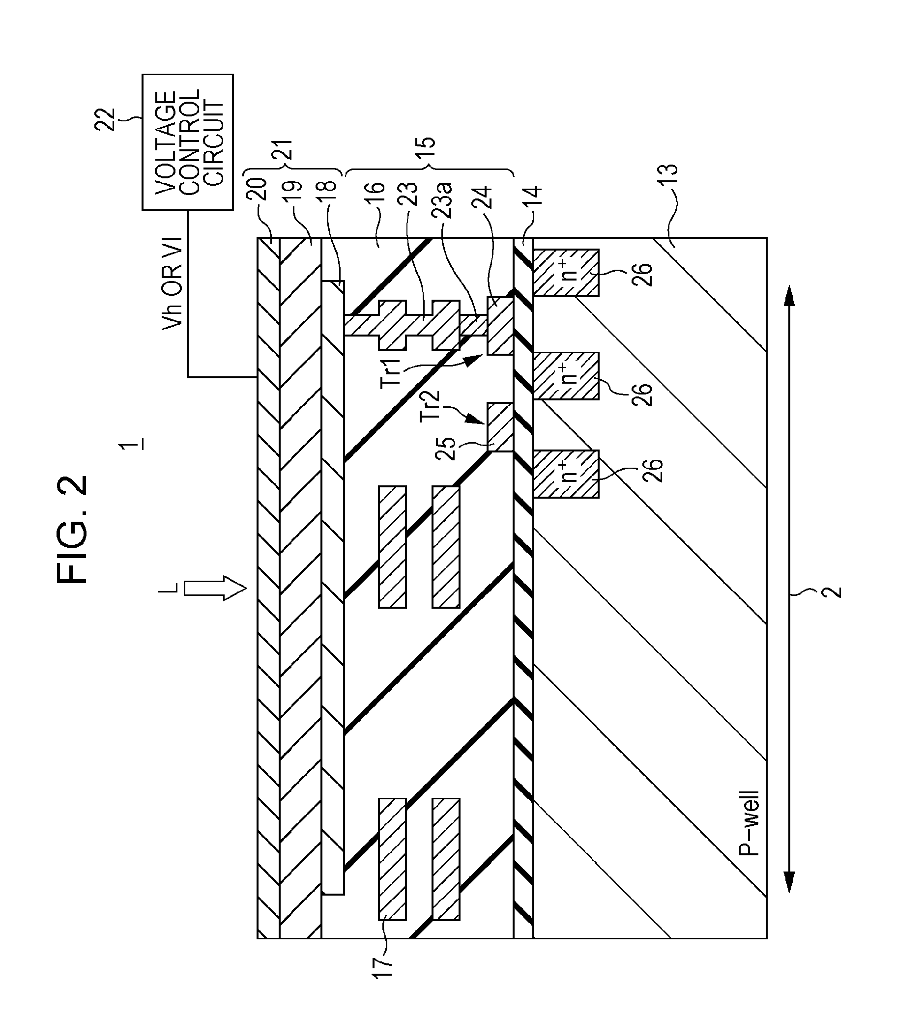
[0058]First, the structure of the solid-state imaging device according to this embodiment, and its fabrication method will be described. FIG. 2 is a schematic cross-sectional diagram (partly in block diagram) of each of the pixels 2 in the solid-state imaging device 1 according to this embodiment.
[0059]Each of the pixels 2 in the solid-state imaging device 1 according to this embodiment has a substrate 13, a wiring layer 15, a photoelectric conversion element 21 provided on top of the substrate 13, and an amplifier transistor Tr1, a select transistor Tr2, and a voltage control circuit 22 which are formed in the substrate 13.
[0060]The substrate 13 is formed by, for example, a silicon substrate of a first conductivity type (hereinafter, referred to as p-type).
[0061]The amplifier transistor Tr1, the select transistor Tr2, and the voltage co...
modification 1
[Modification 1]
[0113]FIG. 7 is a plan diagram of the second electrode 20 with respect to the imaging region according to Modification 1. Modification 1 differs from the first embodiment only in the structure of the second electrode 20.
[0114]In Modification 1, as shown in FIG. 7, the second electrode 20 is formed for each individual row of the pixels 2. The second electrode 20 mentioned above is formed by forming an electrode material on the photoelectric conversion film 19, and then patterning the electrode material.
[0115]In the structure according to Modification 1, the voltage control circuit 22 is connected to each of the second electrodes 20 formed for each individual row, thus enabling control for each individual row. Since Modification 1 allows the second electrodes 20 to be controlled separately for each individual row, there is such an advantage that sensitivity can be adjusted for each individual row.
modification 2
[Modification 2]
[0116]FIG. 8 is a plan diagram of the second electrode 20 with respect to the imaging region 3 according to Modification 2. Modification 2 differs from the first embodiment only in the structure of the second electrode 20.
[0117]In Modification 2, as shown in FIG. 8, the second electrode 20 is formed for each of the individual pixels 2. The second electrode 20 mentioned above is formed by forming an electrode material on the photoelectric conversion film 19, and then patterning the electrode material.
[0118]In Modification 2, the voltage control circuit 22 is connected to each of the second electrodes 20 formed for each of the individual pixels 2, thus enabling control for each of the individual pixels 2. Since Modification 2 allows the second electrodes 20 to be controlled separately for each of the individual pixels 2, there is such an advantage that sensitivity can be adjusted for each of the individual pixels 2.
PUM
 Abstract
Description
Claims
Application Information