Optical imaging device and imaging method for microscopy

a technology of optical imaging and imaging method, which is applied in the field of optical imaging device and imaging method for microscopy, can solve the problems of chromatic aberration, so-called achromatization of such imaging device comprising refractive optical elements, and the elimination of such chromatic aberration, and achieves the effects of low cost, minimum aberration, and high numerical apertur

Active Publication Date: 2014-04-29
CARL ZEISS SMT GMBH
View PDF22 Cites 0 Cited by
  • Summary
  • Abstract
  • Description
  • Claims
  • Application Information

AI Technical Summary

Benefits of technology

[0013]The present invention is based on the cognition that, in a simple manner, with acceptable size of the optical elements used, a high magnification and a high numerical aperture can be in achieved with minimum aberrations if, in a system with two optical element groups each comprising two optical elements, on the one hand, the second optical element group comprises a surface pair of a concave optical surface and a convex optical surface without passage aperture, and, on the other hand, the first optical element group comprises a first optical element with a concave optical surface.
[0014]The design of the second optical element group with a convex optical element without passage aperture, on the one hand, brings the advantage of substantially easier manufacture thanks to the absence of passage aperture. On the other hand, the concave optical surface of the first optical element allows the achievement of a high numerical aperture with small dimensions of the optical elements of the first optical element group. Thus, with the same aspect ratio (ratio of minimum axial thickness to maximum diameter), a smaller working distance from the object can be achieved with a large image field. Furthermore, with such a system, a good image error correction is possible.

Problems solved by technology

A problem here is the chromatic aberrations i.e. the aberrations dependent on the wavelength of the light.
A so-called achromatization of such an imaging device comprising refractive optical elements, i.e. elimination of such chromatic aberrations, is scarcely possible with acceptable cost over a broadband wavelength range (such as that recited above).
The disadvantages of refractive systems described above, however, also apply to such catadioptric systems as known for example from DE 10 2005 056 721 A1 (Epple et al.
The problem with these known catoptric systems, however, is that for a desirably large magnification to be achieved with as few optical elements as possible, in particular, for the optical elements close to the object, comparatively large individual refractive powers are required.
However, in view of the aberrations generated with such catoptric systems, this is disadvantageous so that, frequently, preference is given to the use of more than four mirrors, as it is known from US 2004 / 0114217 A1 (Mann et al.
A further problem in this context is the minimum obscuration at simple manufacture of the imaging device.
Such conical passage apertures are however comparatively complex to produce, so that, as a result, the cost for the imaging device rises considerably.
Here too, the problem is that, on the one hand, a very low numerical aperture (NA=0.3) can be achieved and that the mirror closest to the object again has a very large diameter.

Method used


Image

  • Optical imaging device and imaging method for microscopy
  • Optical imaging device and imaging method for microscopy
  • Optical imaging device and imaging method for microscopy

Examples


Embodiment Construction

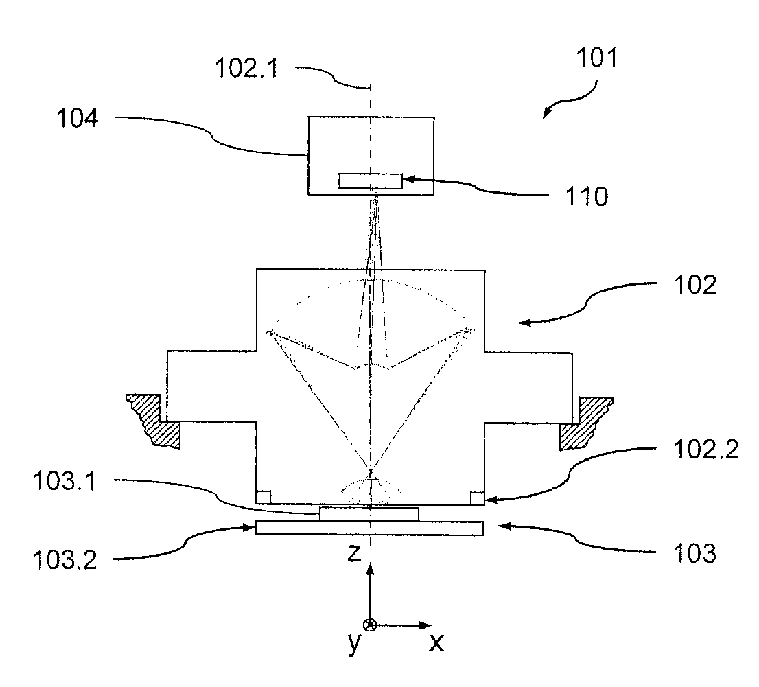
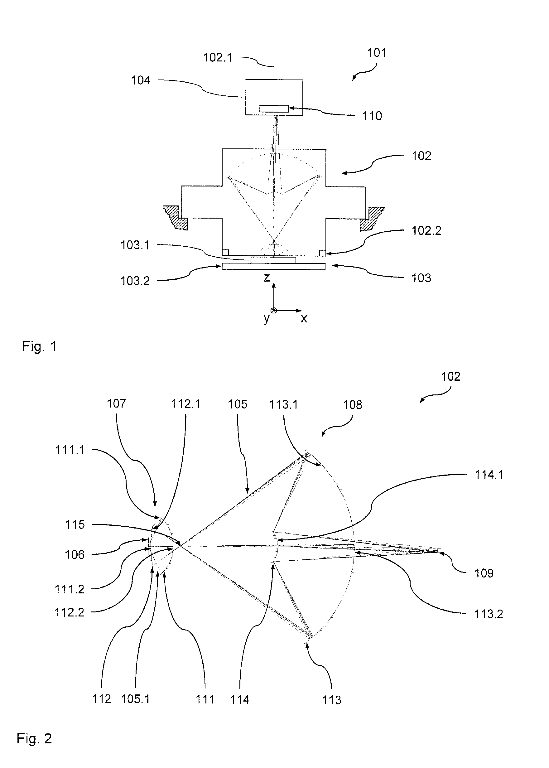
[0024]With reference to FIGS. 1 to 3, a preferred embodiment of the microscope 101 according to the invention comprising a preferred embodiment of the optical imaging device 102 according to the invention is described below.

[0025]In the present example, the microscope 101 is used to inspect the structures formed on a substrate 103.1 (which were produced, for example, via an optical process). However, with other variants of the invention, the microscope according to the invention can also be used for an imaging process in connection with arbitrary applications, in particular, with the inspection of arbitrary other bodies, substrates, surfaces or fluids etc.

[0026]FIG. 1 shows a schematic representation of the microscope 101 which comprises an optical imaging device in the form of an objective 102 (with an optical axis 102.1 and an illumination system 102.2), a substrate device 103 and an image recording device 104. The illumination system 102.2 illuminates (via a light guide device no...


PUM


Abstract

The present invention relates to an optical imaging device, in particular for microscopy, with a first optical element group and a second optical element group, wherein the first optical element group and the second optical element group, on an image plane, form an image of an object point of an object plane via at least one imaging ray having an imaging ray path. The first optical element group comprises a first optical element with a reflective first optical surface in the imaging ray path and a second optical element with a reflective second optical surface in the imaging ray path, wherein the first optical surface is concave. The second optical element group comprises a third optical element with a concave reflective third optical surface in the imaging ray path and a fourth optical element with a convex reflective fourth optical surface in the imaging ray path without light passage aperture.

Description

CROSS-REFERENCE TO RELATED APPLICATIONS[0001]This application claims priority under 35 U.S.C. §119(e)(1) to U.S. Provisional Application No. 61 / 101,485 filed Sep. 30, 2008. This applications also claims priority under 35 U.S.C. §119 to German Patent Application DE 10 2008 049 588.3, filed Sep. 30, 2008. The contents of both of these applications are hereby incorporated by reference in their entirety.BACKGROUND OF THE INVENTION[0002]The present invention relates to optical imaging devices and imaging methods for microscopy. The invention can be applied in connection with the inspection of arbitrary surfaces or bodies.[0003]In many technical areas, it is necessary, among others, to subject bodies and their surfaces to a precise optical inspection in order to be able, for example, to assess the quality of a production process and, where applicable, intervene correctively insofar as the inspection reveals that specified quality criteria are not fulfilled. Naturally, the same if not high...

Claims


Application Information

Patent Timeline
Patent Type & Authority Patents(United States)
IPC IPC(8): G02B21/04
CPCG02B17/0631G02B21/04
Inventor MANN, HANS-JUERGENFELDMANN, HEIKO
Owner CARL ZEISS SMT GMBH
Why Eureka
Try Eureka