Method of cooling electronic circuit boards using surface mounted devices

a technology of electronic circuit boards and surface mounted devices, which is applied in the direction of printed circuit aspects, electrical apparatus contructional details, lighting and heating apparatus, etc., can solve the problems of limited space available on or around the components, higher acoustic noise levels, and the effect of increasing the effective surface of the board

Active Publication Date: 2014-05-20
ADVA OPTICAL NETWORKING SE
View PDF17 Cites 3 Cited by
  • Summary
  • Abstract
  • Description
  • Claims
  • Application Information

AI Technical Summary

Benefits of technology

[0011]The present invention enables electronic circuit boards to be cooled by using distributed small heat sink devices, which are placed or assembled to the board in the form of surface mounted devices (SMD). Since even small spaces on the board (both surfaces) can be filled with heat sink devices (small with dimensions in the range of millimeters, preferably parallelepiped-shaped), it is possible to place such a heat sink device close to a hot spot on the board. A number of heat sink devices, which are mounted directly on the board's surface, increase the effective surface of the board to dissipate heat to the surroundings (improving cooling performance). Since the at least one heat sink device is placed by SMD method, i.e. the device is directly soldered to the board, a good thermal contact between the board and said heat sink device exists.
[0012]The heat sink device according to the invention is defined (when placed on the board) as a non-electrical effective small device (connected to the board with no electrical functions or electrically passive) in contrast to SMD parts like resistors, capacitors, inductors, microprocessors, logical arrays, RAM chip, etc. Such small heat sink device(-s) (compared to lumped heat sink) can be placed near to a (thermal) hot spot on the board. In this manner, it is possible to improve the cooling efficiency, compared to other solutions which are placed remote from a hot spot.
[0013]According to an embodiment of the invention, the heat sink device can be a standard SMD part, like a resistor, inductor, particularly a capacitor. In this embodiment, the standard SMD part does not act as an electrically active resistor, inductor or capacitor. The advantage of using of a standard SMD part as a heat sink device consists in the low costs of these SMD parts (e.g. one-tenth of a cent for a high volume SMS resistor or SMD capacitor per part). Another preferred solution utilizes heat sink devices which are specially produced for the purpose of dissipating heat (away from the board). Since these devices can be optimized (in shape with larger effective surface and thermally conducting material, especially metal such as copper or aluminum) for their thermal (cooling) effect regardless of any electrical function, it is possible to raise the effect of dissipating heat to the surroundings.

Problems solved by technology

Increased temperatures are in fact a main reason for defects of electronic devices.
However, the space available on or around the components is limited in many cases.
Unfortunately, the increased airflow results in higher acoustic noise level and in increased energy costs.
This solution requires an additional mechanical production step with additional costs.
These solutions, however, require an additional mechanical production step with additional costs.
Unfortunately, in many cases, this results in a certain distance between the hot spot and such lumped heat sink, which decreases the effect of dissipating heat from the board.
Moreover, in many cases, the space available is limited and the use of a lumped heat sink is not possible.
However, in the layout of some boards, there is not even enough room or space on the board to place further fans or cooling units.
Unfortunately, this solution is quite expensive and is not available from every board manufacturer.

Method used


Image

  • Method of cooling electronic circuit boards using surface mounted devices
  • Method of cooling electronic circuit boards using surface mounted devices
  • Method of cooling electronic circuit boards using surface mounted devices

Examples


first embodiment

[0050]In a first embodiment shown in FIG. 3 to FIG. 6, the solder pads 26, 28 are also (thermally) connected to a first 27, second 29, third 31, fourth 33 and bottom layer 35 by means of through holes 21 and 22.

second embodiment

[0051]In a second embodiment shown in FIG. 7 to FIG. 10 (as an example of being connected to one or more layers), the solder pads 26, 28 are only (thermally) connected to the first layer 27 by means of microvias 21′ and 22′ without any connection to the other layers 29, 31, 33 and 35.

[0052]Of course, the heat sink device 1′ can be connected via solder pads 26, 28 to circuits on the top face in both embodiments only or to any combination of layers as required or possible during the layout of the board.

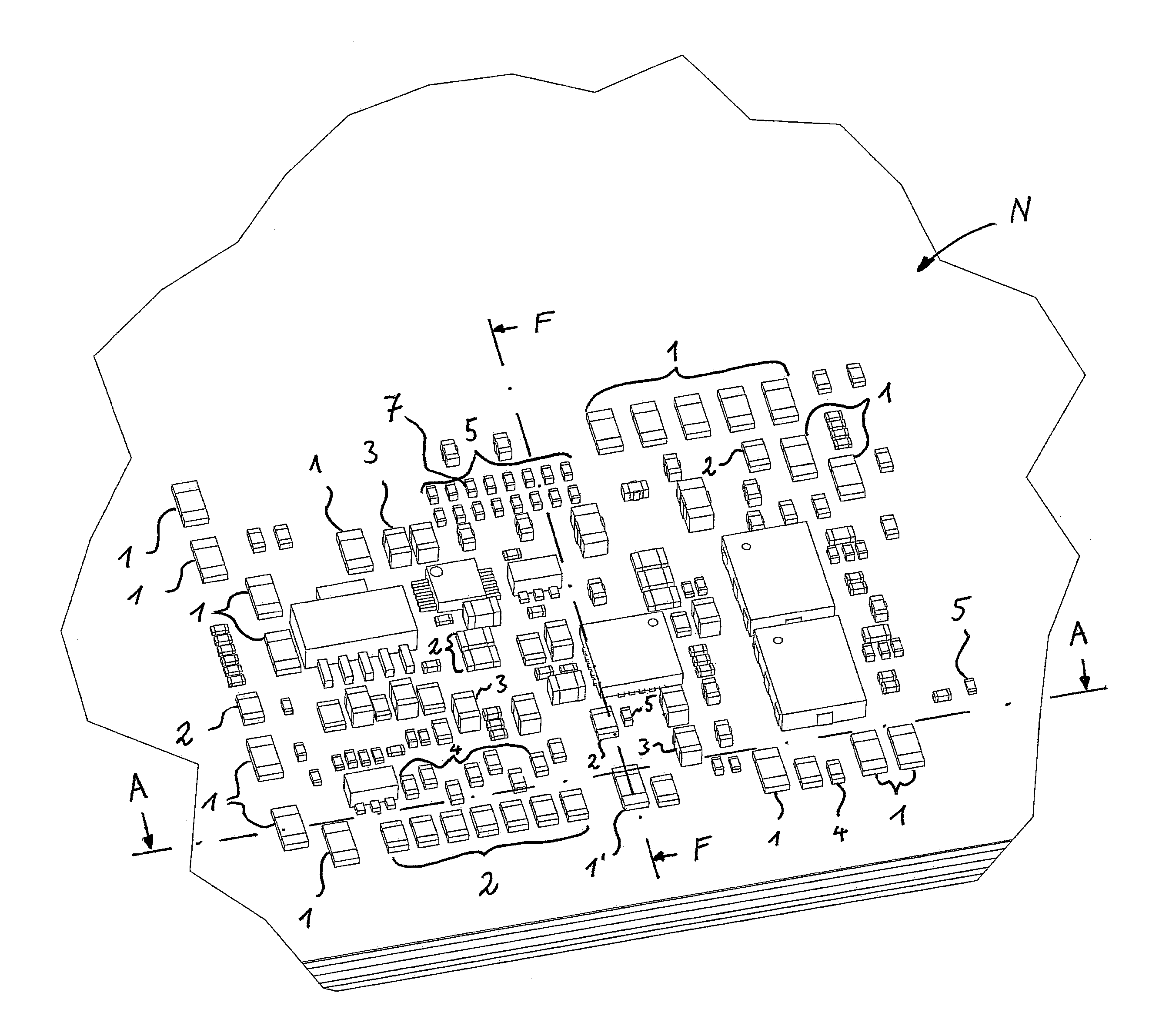
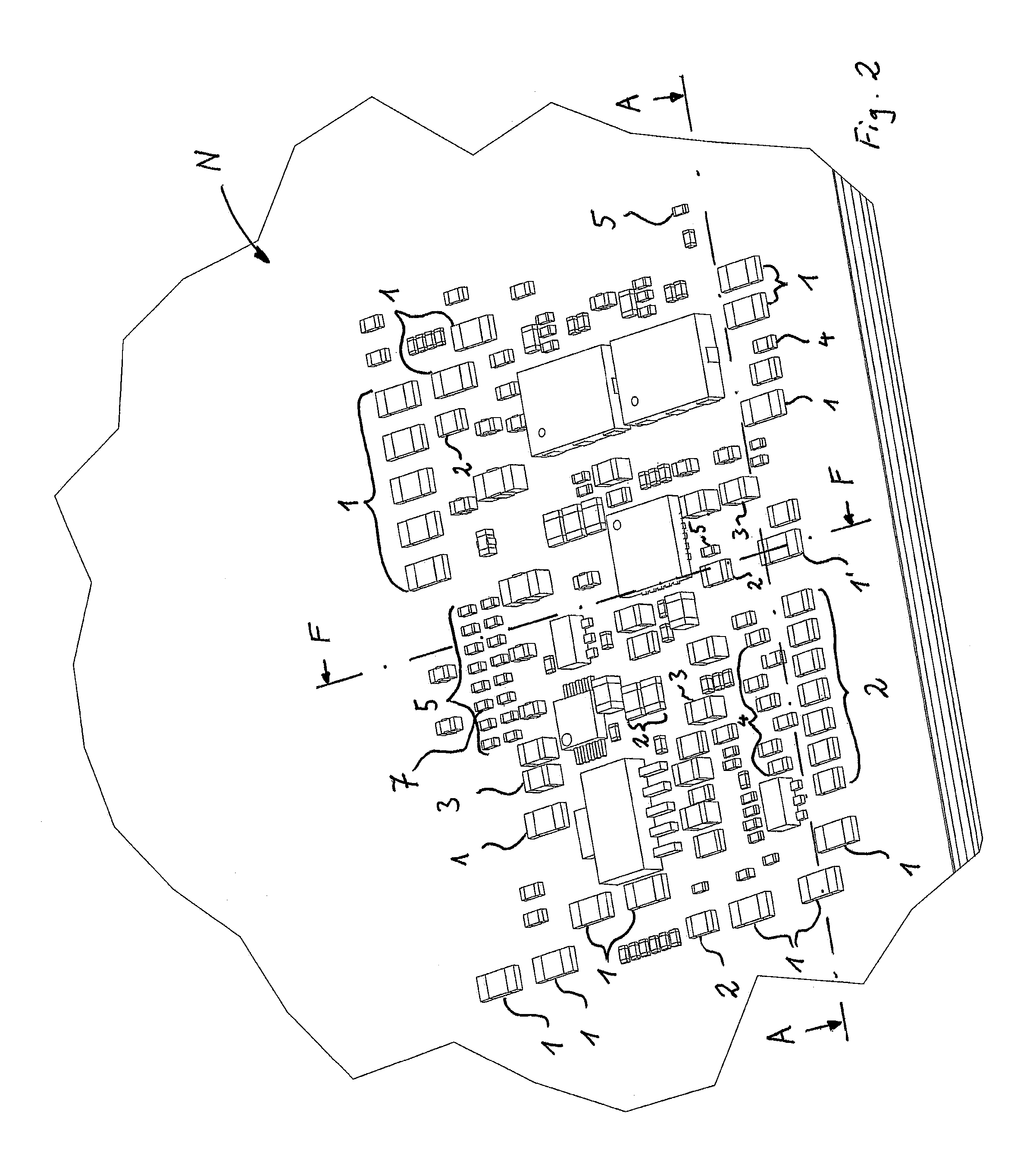
[0053]The heat sink devices 1, 2, 3, 4, 5 distributed on the printed circuit board N filling free spaces (places in the board layout without any electrically functional SMD device) act as a distributed heat sink cooling the board. Therefore, the heat sink devices are connected to one layer, particulary the top face 25 or to any combination of layers 25, 27, 29, 31, 33 and 35 of the board N.

[0054]In this way, it is possible to improve the cooling performance of the board without increasi...


PUM


Abstract

The invention relates to a method of cooling electronic circuit boards using surface mounted devices (SMD), the method comprising the steps of: after or during the board layout, filling empty spaces V1, V2, V3, V4, V5, V6, V7, V8, V9, V10 with at a number of heat sink devices 1, 2, 3, 4, 5 near a thermal hot spot and connecting the number of heat sink devices 1, 2, 3, 4, 5 to a thermally conducting path 25, 27, 29, 31, 33, 35 of the board N, respectively. Further, the invention relates to a heat sink device 1, 2, 3, 4, 5 adapted to implement the method according to the invention.

Description

BACKGROUND OF THE INVENTION[0001]1. Field of the Invention[0002]The invention relates to a method of cooling electronic circuit boards using surface mounted devices. Further, the invention relates to a heat sink device for cooling electronic circuit boards using surface mounted devices.[0003]2. Description of Related Art[0004]In most electronic circuit boards, temperature results from the electronic function of the board, or rather the electronically active parts on the board. Increased temperatures are in fact a main reason for defects of electronic devices.[0005]Temperature-critical applications use lumped heat sinks to reduce the temperature of the electronic components. However, the space available on or around the components is limited in many cases.[0006]A known method of cooling electronic circuit boards, which surface mounted devices are placed on, uses a fan to increase the airflow. Unfortunately, the increased airflow results in higher acoustic noise level and in increased...

Claims


Application Information

Patent Timeline
Patent Type & Authority Patents(United States)
IPC IPC(8): H05K7/20
CPCH05K3/341H05K2201/10204H05K2201/066H05K1/0209H05K1/0207Y10T29/49155
Inventor WALD, TONILIBORIUS, SVEN
Owner ADVA OPTICAL NETWORKING SE
Why Eureka
Try Eureka