DC-DC converter vertically integrated with load inductor structured as heat sink

a load inductor and vertical integration technology, applied in the direction of heat transfer modification, magnetic bodies, instruments, etc., can solve the problems of reducing the efficiency of the converter, reducing the integration of the inductor with the fets, and reducing the pcb area required for assembly and associated parasitic losses, so as to reduce the pbc area required for assembly and the associated parasitic losses, enhancing the converter efficiency, and reducing parasitic resistance and inductan

Active Publication Date: 2014-06-24
TEXAS INSTR INC
View PDF8 Cites 3 Cited by
  • Summary
  • Abstract
  • Description
  • Claims
  • Application Information

AI Technical Summary

Benefits of technology

[0009]Applicant solved the problem of reducing the PBC area required for assembly and the associated parasitic losses by shaping the load inductor to double as an effective heat sink. The inventive concept includes a vertical stacking of the load inductor over the switch node plate carrying the FETs so that the load current is guided along the FETs and through the inductor; the current-generated heat is channeled through a thick heat-spreading copper sleeve wrapped around the inductor and in touch with the plate into the heat capacity of the ferrite core and especially into the ambient.
[0010]As a consequence of this arrangement, the load inductor is integrated with the FETs, saving the valuable PCB assembly area, and the integration is not passive but active since the inductor participates as heat spreader and heat sink to enhance the converter efficiency.
[0011]The implementation which embodies the inventive principle is an assembly methodology which first attaches side-by-side a first FET drain-down and a second FET source-down onto a first surface of a conductive carrier as switch node. In the next step, a thermally conducting copper sleeve is wrapped around the encapsulation of the inductor having a ferrite core. Then, the copper-wrapped inductor is aligned with the opposite carrier surface vertically above FETs, and the sleeve is soldered onto carrier. As a side benefit of this methodology, short and tight current loops are created for a load filter capacitor and an input capacitor, reducing parasitic resistance and inductance.
[0012]The stacking of the load inductor on top of the FETs reduces about 50% of the consumed PCB area compared to conventional side-by-side placement. This vertical integration enables very short interconnects and circuit loops to reduce parasitic resistances and inductances, and thus to improve power density, efficiency, and switching transients (“ringing”). The morphing of the load inductor into a heat sink enables higher switching currents before the allowed 150° C. junction temperature is reached; as an example, currents up to 35 A can now be handled at 500 to 2000 kHz instead of the conventional 25 A. Further, reduced operating temperature enables higher speed of the DC-DC converter and thus higher efficiency.

Problems solved by technology

This arrangement consumes increasingly valuable PCB area.
Further, the PCB traces necessary to connect the FETs and the inductor introduce parasitic resistances and inductances, which reduce the converter efficiency.
Analyzing the options for reducing the required PBC assembly area and associated parasitic losses, applicants found that an integration of the inductor with the FETs is impeded not only by the bulky dimensions of the inductor, but also by its irregular and large heat capacitance due to its composition of copper wires surrounded by magnetic ferrite material; the heat capacitance disturbs the action of a comb added to the FETs as a heat sink.

Method used


Image

  • DC-DC converter vertically integrated with load inductor structured as heat sink
  • DC-DC converter vertically integrated with load inductor structured as heat sink
  • DC-DC converter vertically integrated with load inductor structured as heat sink

Examples


Embodiment Construction

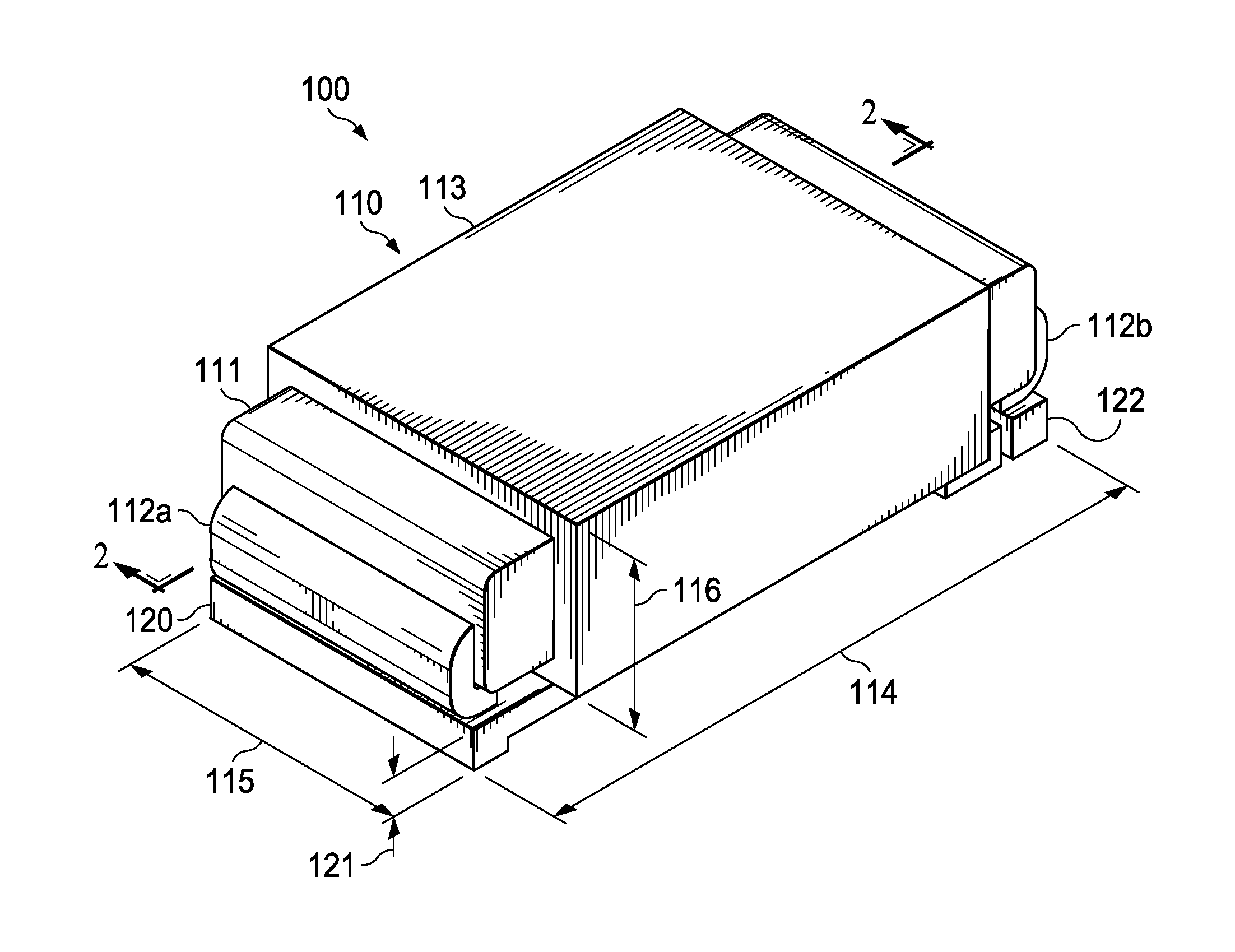
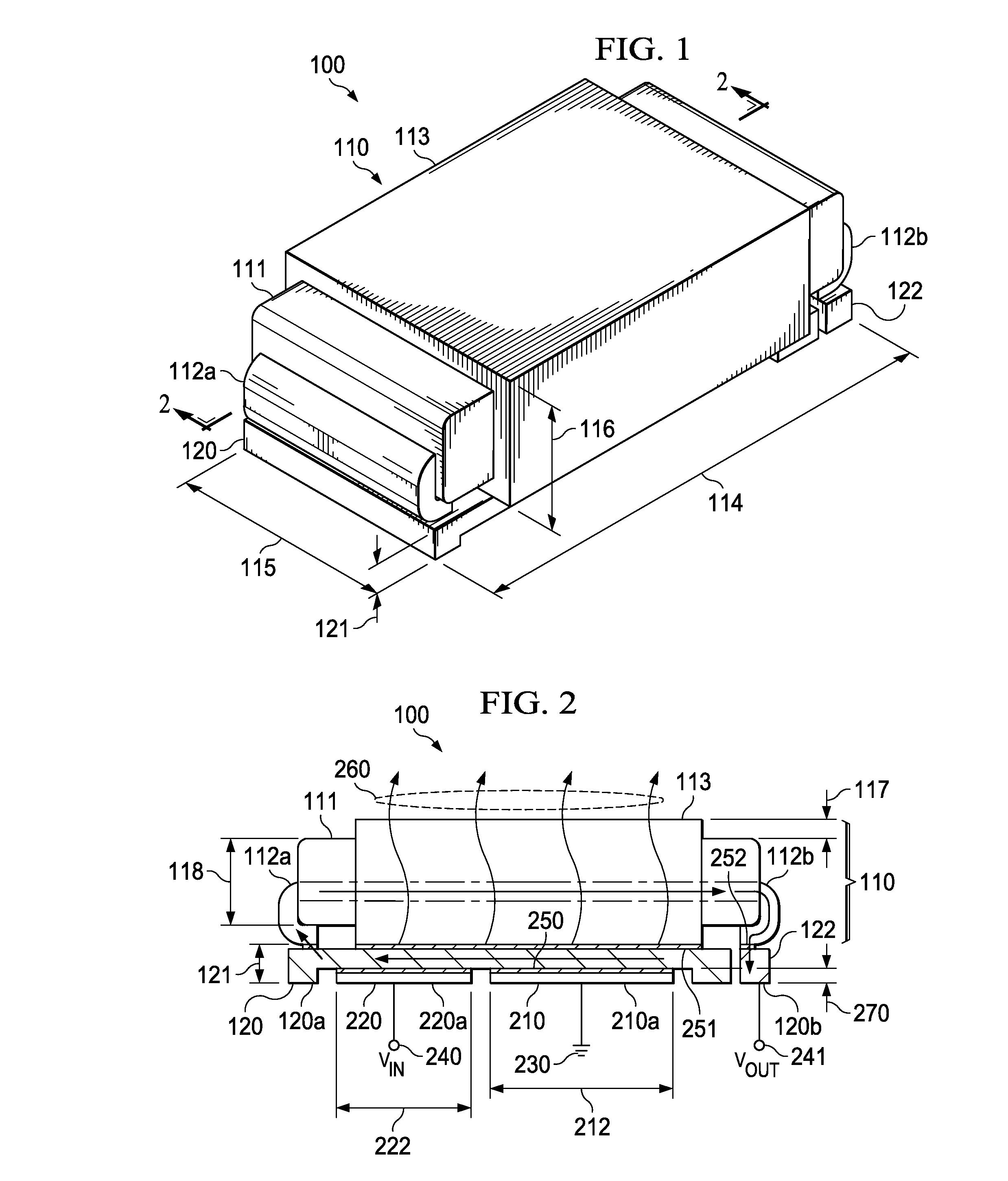
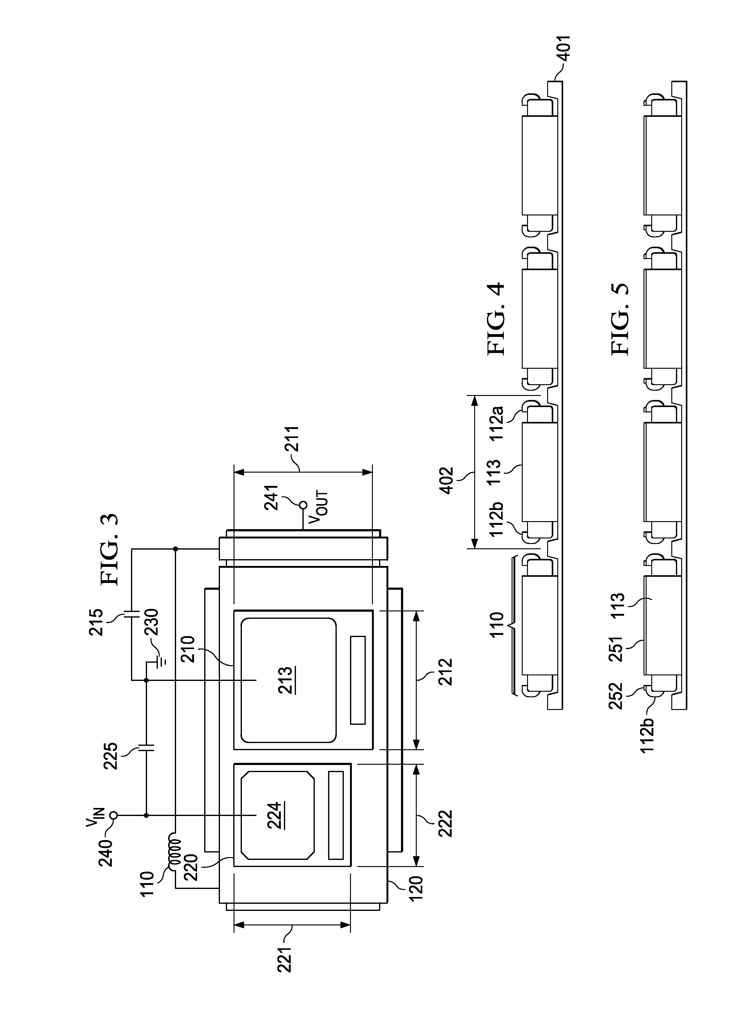
[0022]FIG. 1 shows a perspective top view of an exemplary finished power converter, generally designated 100, with the load inductor 110 vertically integrated with conductive carrier 120, acting as the switch node of the field effect transistors (FETs) (not visible in FIG. 1) of a half-bridge, or synchronous Buck converter. The visibly dominating features of load inductor 110 include housing 111, the leads 112a and 112b to the metal coil inside the ferrite, and the metal sleeve 113 wrapped around the length of the housing. Lead 112b is attached to output terminal 122, which is separated from carrier 120 but made from the same metal sheet (see FIG. 6).

[0023]Generally, an inductor such as load inductor 110 includes inside a spirally configured coil of coated metal wire, preferably copper, welded to a plated leadframe, also preferably copper, and molded into a magnetic ferrite material, often called ferrimagnetic in short. The ferrite material is pressed at high pressure, cured, and en...


PUM

PropertyMeasurementUnit
heightaaaaaaaaaa
heightaaaaaaaaaa
side lengthaaaaaaaaaa

Abstract

A power supply converter (100) comprising a first FET (210) connected to ground (230), the first FET coupled to a second FET (220) tied to an input terminal (240), both FETs conductively attached side-by-side to a first surface of a metal carrier (120) and operating as a converter generating heat; and a packaged load inductor (110) tied to the carrier and an output terminal (241), the inductor package wrapped by a metal sleeve (113) in touch with the opposite surface of the metal carrier, the sleeve operable to spread and radiate the heat generated by the converter.

Description

FIELD OF THE INVENTION[0001]The present invention is related in general to the field of semiconductor devices and processes, and more specifically to structure and fabrication method of a multi-component electronic system including a load inductor structured as a heat sink and vertically integrated with a DC-DC converter half-bridge.DESCRIPTION OF RELATED ART[0002]Electronic products in commercial applications such as telecom, home audio, and regulator products often need systems, which can switch power supplies, regulate and stabilize voltages, and work as dc-dc converters. These systems not only need to have high efficiency to operate properly, but should preferably also have small lateral and thickness dimensions, and require very low cost.[0003]As an example of a system, popular power switches involve a rectangular metal leadframe of 15 by 9 mm outline, on which a plurality of discrete electronic components are assembled and then, as a unit, overmolded with a plastic encapsulati...

Claims


Application Information

Patent Timeline
Patent Type & Authority Patents(United States)
IPC IPC(8): H05K7/20
CPCH02M3/00H01R43/26H05K7/209H02B1/48H05K7/2089H05K7/2039Y10T29/49002Y10T29/49117Y10T29/49073H01F27/22H02M3/003
Inventor HERBSOMMER, JUAN A.LOPEZ, OSVALDO JNOQUIL, JONATHAN AJAUREGUI, DAVIDHRISCU, LUCIAN
Owner TEXAS INSTR INC
Why Eureka
Try Eureka