
Static timing analysis with design-specific on chip variation de-rating factors

a timing analysis and design-specific technology, applied in the field of timing analysis of integrated circuit designs, can solve the problems of inability to run the computer, the integrated circuit designer may not be familiar with ssta tools, and the tool life may be longer, so as to reduce the run time of timing analysis

Inactive Publication Date: 2014-06-24
CADENCE DESIGN SYST INC
View PDF10 Cites 6 Cited by
  • Summary
  • Abstract
  • Description
  • Claims
  • Application Information

AI Technical Summary

Benefits of technology

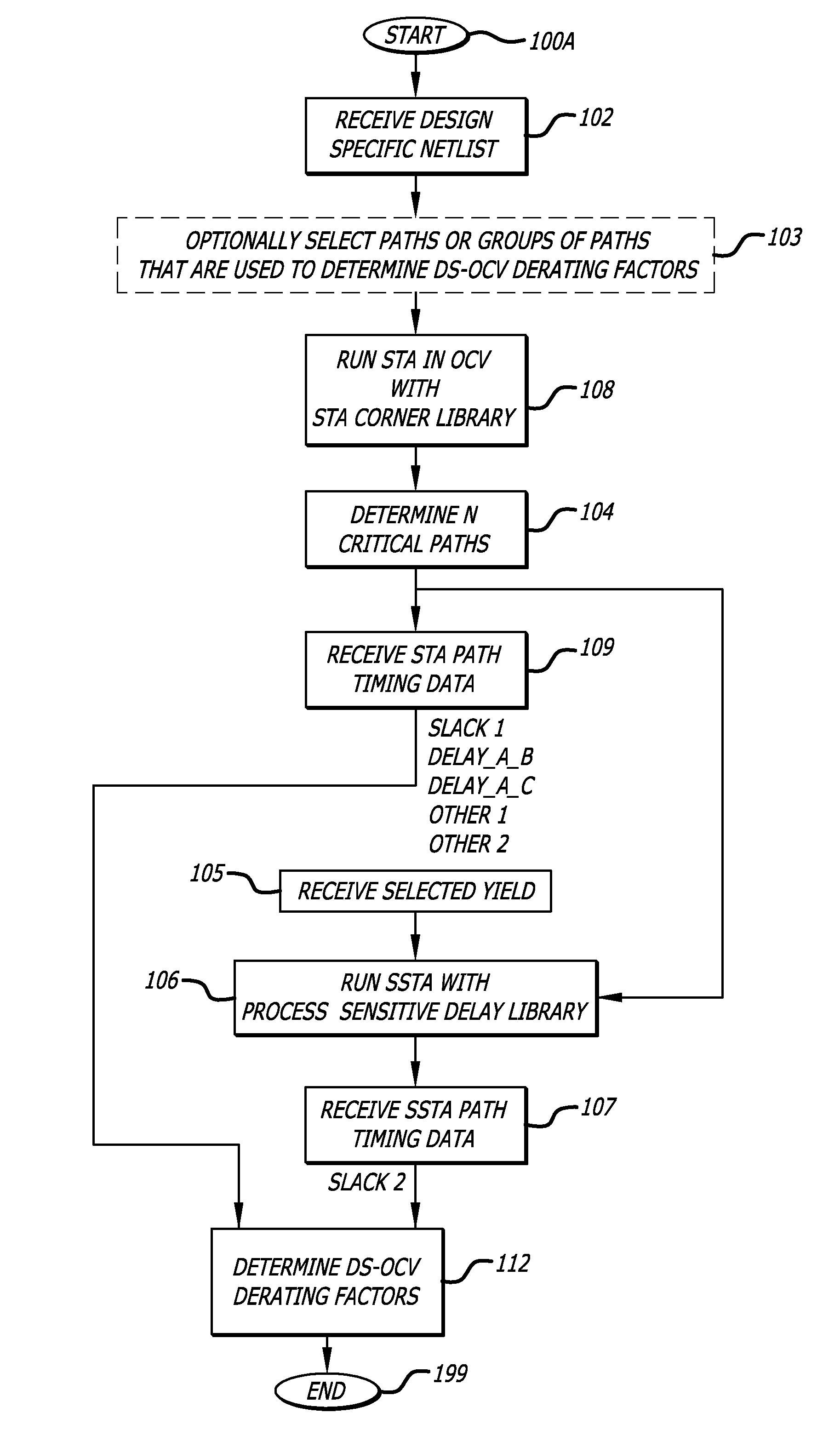
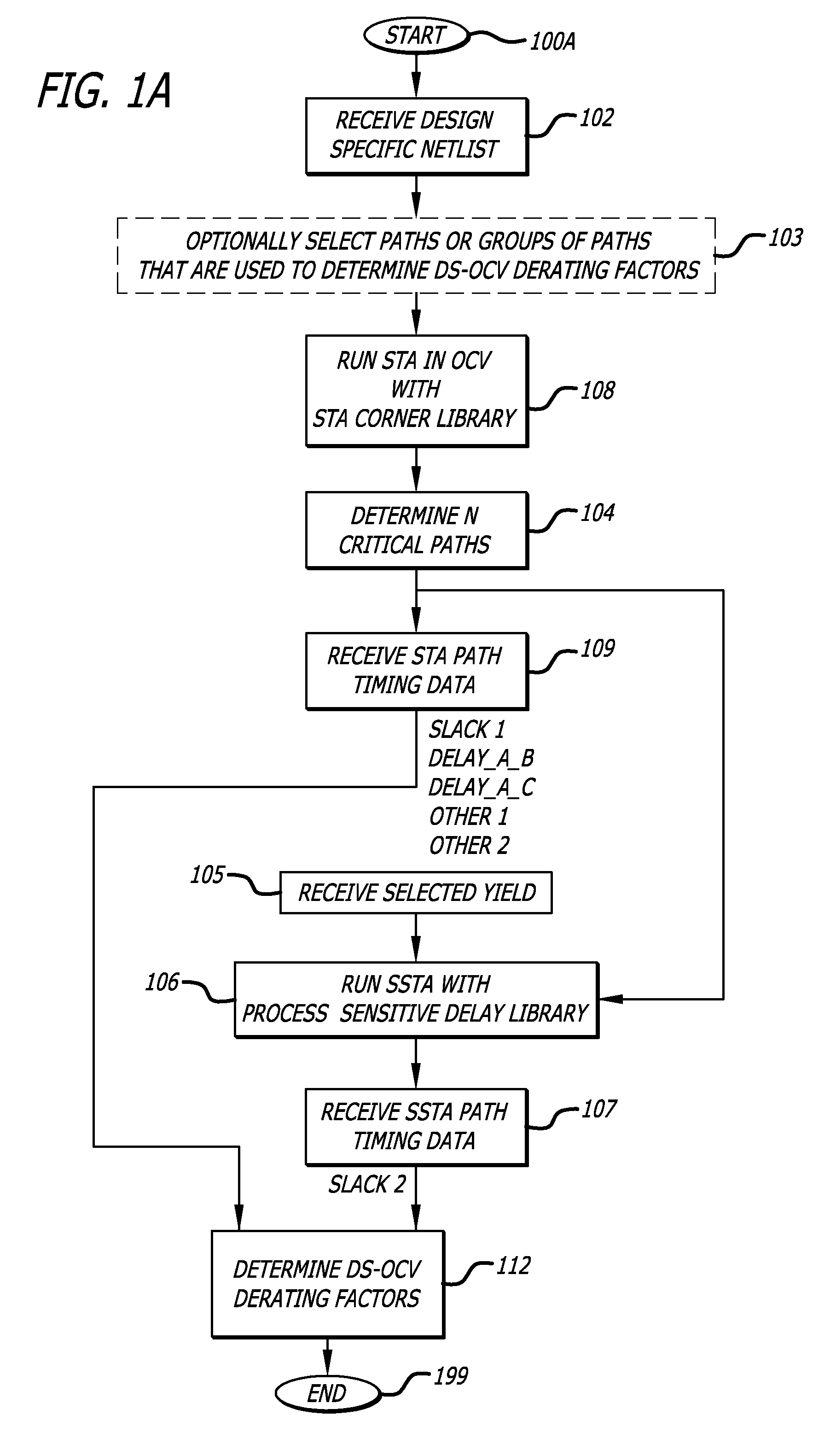
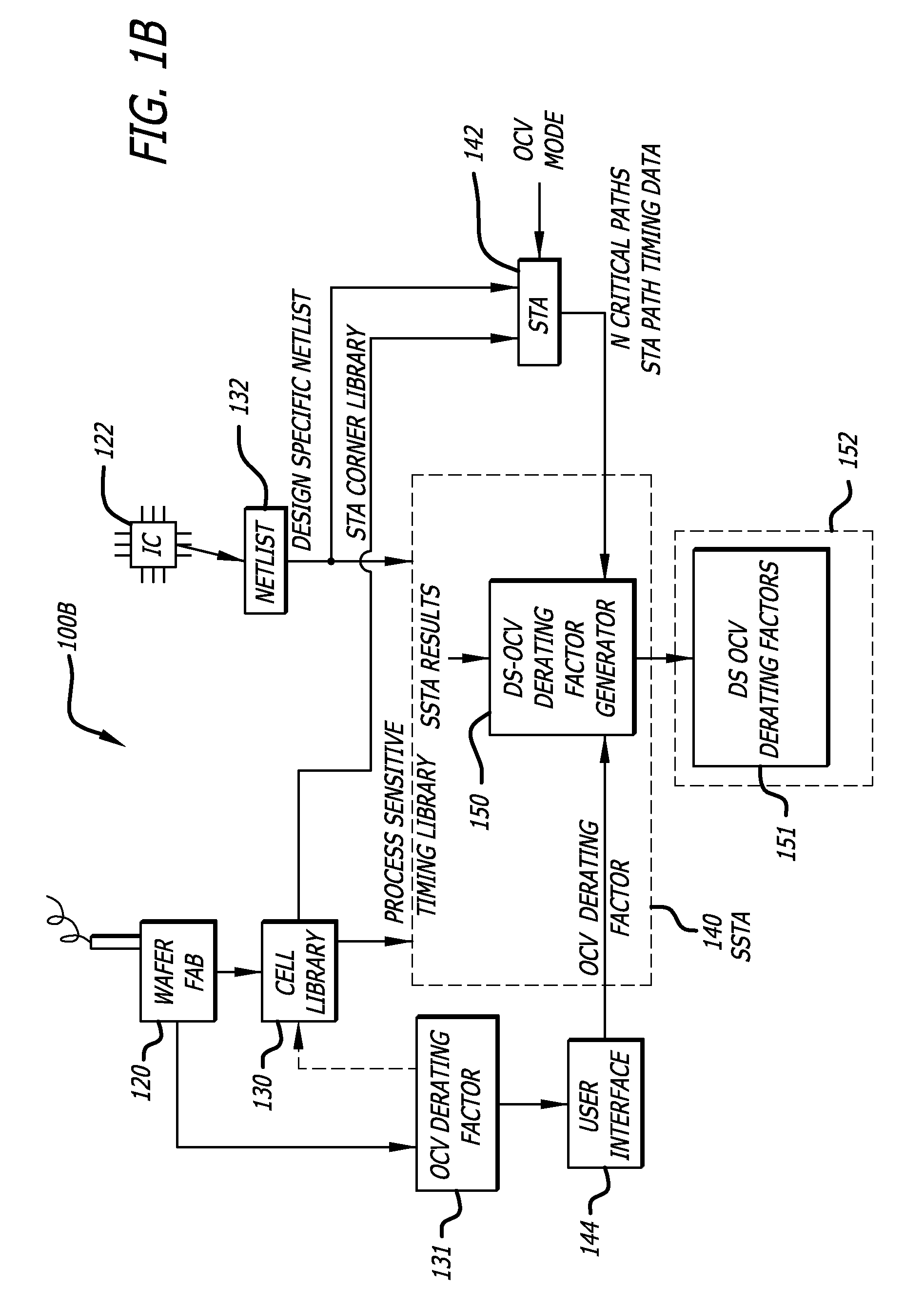
The patent describes a method for analyzing a circuit design to account for changes in the manufacturing process. This method involves performing a static timing analysis (STA) and a statistical static timing analysis (SSTA) on a subset of paths in the design. By comparing the results of these analyses, the method calculates "de-rating factors" that can be used to make a more accurate timing analysis of all paths in the circuit design. This reduces the time required for a full timing analysis.

Problems solved by technology

However, fabrication technology advances have increased the significance of process variations on circuits such that not all process variations can be accounted for using this approach.
STA tools typically trade off accuracy in the results to reduce the computer run-time necessary to achieve those results.
However, integrated circuit designers may be less familiar with SSTA tools.
The setup / integration time to implement SSTA tools may be longer, run-time may be longer without computer performance improvements, and the results tend to be more complicated and difficult to analyze.
However, not accounting for on chip variation and / or design specific process sensitivity could impact the functionality, integrated circuit size, and performance.

Method used


Image

  • Static timing analysis with design-specific on chip variation de-rating factors
  • Static timing analysis with design-specific on chip variation de-rating factors
  • Static timing analysis with design-specific on chip variation de-rating factors

Examples


Embodiment Construction

[0018]In the following detailed description of the embodiments of the invention, numerous specific details are set forth in order to provide a thorough understanding of the embodiments of the invention. However, it will be obvious to one skilled in the art that the embodiments of the invention may be practiced without these specific details. In other instances well known methods, procedures, components, and circuits have not been described in detail so as not to unnecessarily obscure aspects of the embodiments of the invention.

[0019]The embodiments of the invention include a method and system to statically analyze timing for design-specific on chip variations (DS-OCV).

Variations that Influence Timing

[0020]Variations that effect timing characteristics of an integrated circuit can broadly be categorized into two classes, process variations and environmental variations. Process variations result from perturbations in the fabrication process that change the values of parameters such as ...


PUM


Abstract

In one embodiment of the invention, a method of analysis of a circuit design with respect to within-die process variation is disclosed to generate a design-specific on chip variation (DS-OCV) de-rating factor. The method includes executing a static timing analysis (STA) in an on-chip variation mode using a process corner library. Collecting timing information of the top N critical timing paths. Executing a statistical static timing analysis (SSTA) on the N critical timing paths using timing models characterized for SSTA with sensitivities of delays to process variables. Compare the two timing results and deriving DS-OCV de-rating factors for the clock / data paths to be used in a STA OCV timing analysis to correctly account for the effects of process variations. A user may select to specify DS-OCV de-rating factors for paths or groups of paths and achieve an accurate timing analysis report in a reduced amount of run-time.

Description

CROSS REFERENCE TO RELATED APPLICATIONS[0001]This application claims the benefit of U.S. Provisional Application No. 61 / 267,010; entitled DESIGN-SPECIFIC ON CHIP VARIATION DE-RATING FACTORS FOR STATIC TIMING ANALYSIS OF INTEGRATED CIRCUITS; filed on Dec. 4th, 2009 by inventors Hongliang Chang et al.FIELD[0002]The embodiments of the invention relate generally to timing analysis of integrated circuit designs.BACKGROUND[0003]Semiconductor fabrication and manufacturing technologies continue to advance and allow an increase in the number of integrated circuits on a die and across a wafer. Identical circuits on a wafer or within the same die may have different performance characteristics due to fabrication or manufacturing process variations.[0004]Some of the fabrication or manufacturing process variations can be accounted for by using a corner-based static timing analysis approach. The fabrication processes can be characterized by running test chips, circuits designed to capture the proc...

Claims


Application Information

Patent Timeline
Patent Type & Authority Patents(United States)
IPC IPC(8): G06F9/455G06F17/50
CPCG06F17/504G06F2217/84G06F30/3323G06F2119/12
Inventor CHANG, HONGLIANGGEROUSIS, VASSILIOSMOLAKALAPALLI, SIREESHASHRIVASTAVA, SACHIN
Owner CADENCE DESIGN SYST INC
Learn More