Repaired organic EL display and method for manufacturing same including repairing process

a technology of organic el and display, which is applied in the field of organic el display, can solve the problems of low luminous efficiency, current leakage between the electrodes via foreign material, and inability to completely rid the clean room of foreign materials, so as to prevent brightness variation and prevent brightness reduction

Active Publication Date: 2014-07-08
JOLED INC
View PDF18 Cites 3 Cited by
  • Summary
  • Abstract
  • Description
  • Claims
  • Application Information

AI Technical Summary

Benefits of technology

[0043]With the manufacturing method of organic EL display of the present invention, it is possible to prevent brightness reduction in a non-luminescent region because a portion of a color filter directly above the non-luminescent region is also ablated, thus preventing brightness variation across the organic EL display (later described).

Problems solved by technology

Nevertheless, it is not possible to completely rid the clean room of foreign material such as particles derived from an organic layer manufacturing machine or other device or from the surrounding environment.
When voltage is applied between the pixel electrode and counter electrode in a state where an organic layer is contaminated with foreign material, it results in current leakage between the electrodes via the foreign material.
Current leakage results in low luminous efficiency, leading to high power consumption.
Moreover, in a pixel contaminated with foreign material, current leakage via the foreign material reduces the current flow in the organic layer (light-emitting layer) of the pixel.
This reduces the overall brightness of the light-emitting layer of the pixel.

Method used


Image

  • Repaired organic EL display and method for manufacturing same including repairing process
  • Repaired organic EL display and method for manufacturing same including repairing process
  • Repaired organic EL display and method for manufacturing same including repairing process

Examples


embodiment 1

[0101]Embodiment 1 describes a case where the third step and the color filter ablation step (filter ablation step) are the same step.

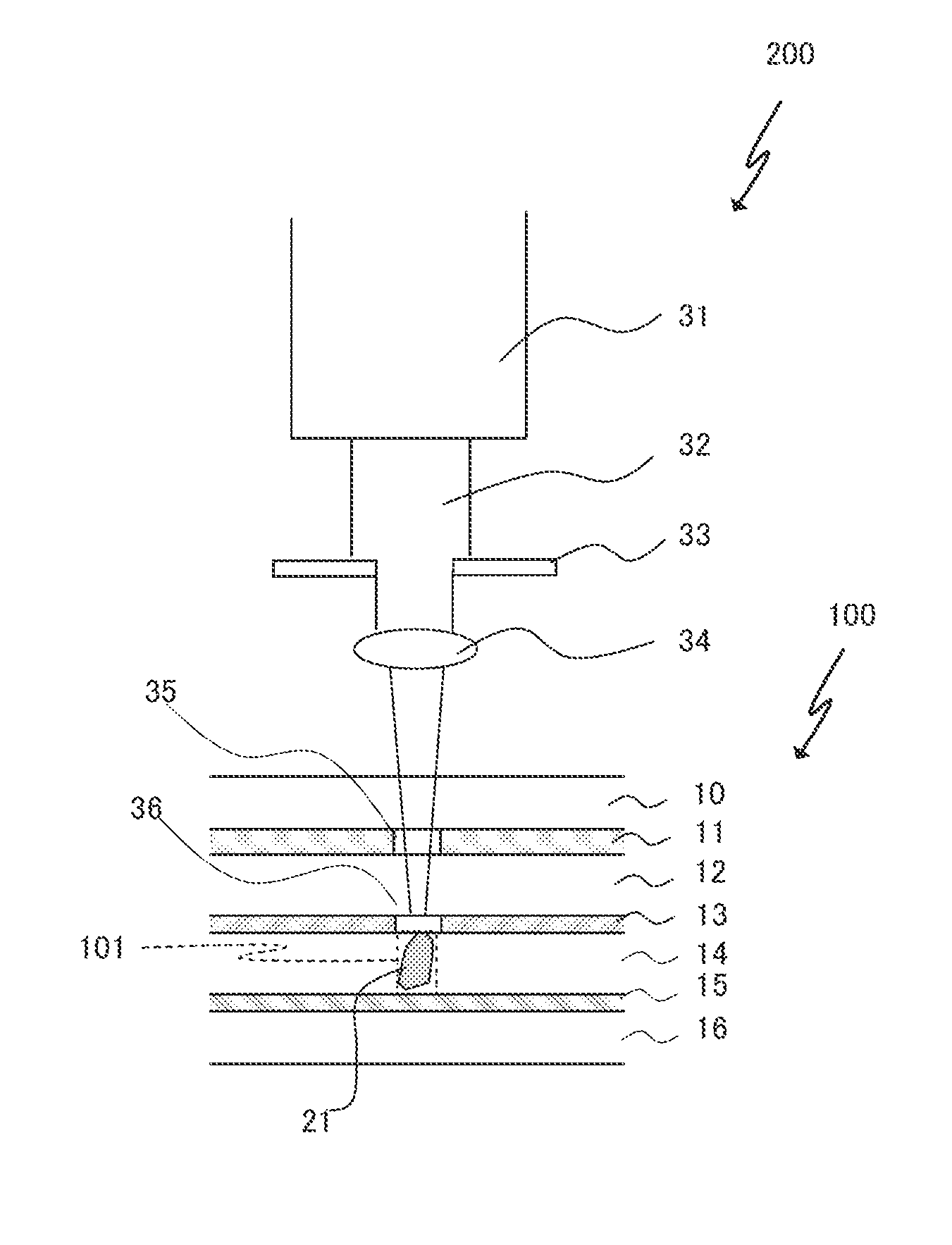
[0102]FIG. 3A illustrates organic EL device 100 having a defect detected in the second step (step of detecting a defect in the organic layer of an organic EL device) of the manufacturing method of the present invention.

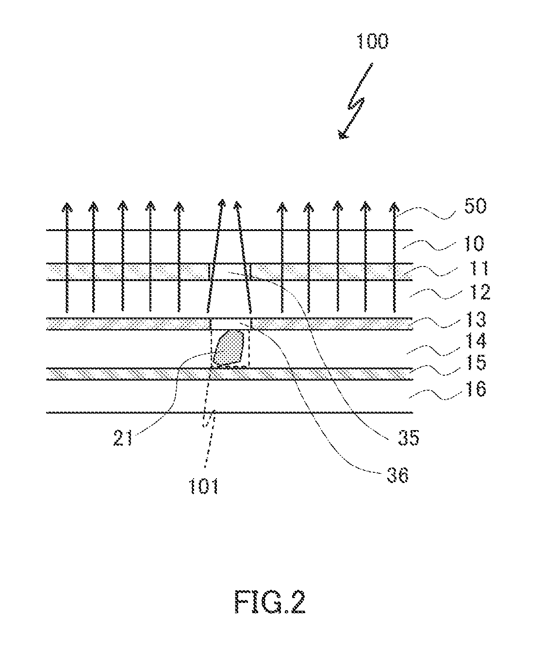
[0103]Organic EL device 100 of FIG. 3A includes substrate 16, pixel electrode 15, organic layer 14, transparent counter electrode 13, protective layer 12, color filter 11, and sealing glass 10. Organic layer 14 has foreign material 21, and the region of organic layer 14 contaminated with foreign material 21 constitutes defect 101.

[0104]On the other hand, the organic EL display of the present invention also includes organic EL device 103 free of any defect, such as that illustrated in FIG. 3B.

[0105]FIG. 4 illustrates a third step and a filter ablation step according to Embodiment 1. As illustrated in FIG. 4, laser device 200 used in the t...

embodiment 2

[0111]Embodiment 1 describes a case where the third step and filter ablation step are the same step. Embodiment 2 describes a case where the third step and filter ablation step are different steps.

[0112]FIG. 5A illustrates a filter ablation step according to Embodiment 2. FIG. 5B illustrates a third step according to Embodiment 2.

[0113]As illustrated in FIG. 5A, in the filter ablation step according to this embodiment, laser beam 32 is first focused onto a portion of color filter 11 directly above defect 101, ablating the irradiated portion of color filter 11 to form through-hole 35. Laser beam 32 with a specific wavelength that cannot pass through color filter 11 is focused onto color filter 11.

[0114]For example, in the case where flash lamp-pumped Nd:YAG laser is employed as laser source 31, when color filter 11 is red, the wavelength of laser beam 32 may be set to 532 nm (second harmonics) while setting the laser energy density on color filter 11 to 0.48 J / cm2 or greater, or the ...

embodiment 3

[0117]Embodiments 1 and 2 both describe a case where a laser-irradiated portion of a color filter is completely ablated to form a through-hole therein. Embodiment 3 describes a case where a laser-irradiated portion of a color filter is not completely ablated.

[0118]FIG. 6A illustrates a filter ablation step according to Embodiment 3. FIG. 6B illustrates a third step according to Embodiment 3.

[0119]As illustrated in FIG. 6A, in the filter ablation step according to this embodiment, laser beam 32 is first focused onto a portion of color filter 11 directly above defect 101, ablating the surface of the laser-irradiated portion of color filter 11 for thinning region 40 of color filter 11. This embodiment is characterized in that the wavelength or energy density of laser beam 32 is adjusted such that the laser-irradiated portion of color filter 11 is not completely ablated.

[0120]Subsequently, in the third step, laser beam 32 is focused onto a portion of transparent counter electrode 13 dir...


PUM


Abstract

Disclosed is a method for manufacturing an organic EL display, which comprises: a step of preparing an organic EL panel that comprises a substrate and organic EL elements arranged as a matrix on the substrate, wherein each organic EL element has a pixel electrode arranged on the substrate, an organic layer arranged on the pixel electrode, a transparent counter electrode arranged on the organic layer, a protective layer arranged on the transparent counter electrode, and a color filter arranged on the protective layer, and a defect portion present in the organic layer in each organic EL element is detected; a step of destroying a region of the transparent counter electrode positioned above the defect portion by irradiating the region with laser light through the color filter; and a step wherein a region of the color filter positioned above the defect portion is removed.

Description

TECHNICAL FIELD[0001]The present invention relates to an organic EL display and a manufacturing method for the same.BACKGROUND ART[0002]Recently, organic EL displays have attracted attention as the next-generation flat display panels. The organic EL displays have such advantages as self-luminescence, wide viewing angle, high-contrast image, thin profile, lightweight, and low power consumption.[0003]Each of the organic EL devices that constitute an organic EL display generally includes a pixel electrode, a counter electrode, and an organic layer disposed between the pixel electrode and counter electrode. The organic layer is composed of a light-emitting layer containing fluorescent molecules, and an electron conductive thin film and a hole conductive thin film which sandwich the light-emitting layer. Application of voltage between the counter electrode and the pixel electrode results in the injection of electrons into the electron conductive thin film from the counter electrode and i...

Claims


Application Information

Patent Timeline
Patent Type & Authority Patents(United States)
IPC IPC(8): H01L21/00H01L27/32H01L51/52
CPCH01L27/3281H01L27/322H01L51/5206H01L51/5221H01L51/56H01L2251/5315H01L2251/568H05B33/10H05B33/26H05B33/28Y10S438/94H01L51/5234H10K59/38H10K50/818H10K50/828H10K2102/3026H10K71/861H10K71/00H10K59/17H10K50/82
Inventor MIYAZAWA, KAZUTOSHINAKAHASHI, AKIHISA
Owner JOLED INC
Why Eureka
Try Eureka