
Manufacturing methods for accurately aligned and self-balanced superjunction devices

a manufacturing method and superjunction technology, applied in the direction of semiconductor devices, electrical apparatus, transistors, etc., can solve the problems of limited practical application and usefulness of high-voltage semiconductor power devices, difficulties and limitations of conventional manufacturing techniques, and achieve accurate control of the critical dimension of the doped region, and reduce the variation of charges in the doped region

Active Publication Date: 2014-07-22
ALPHA & OMEGA SEMICON INC
View PDF10 Cites 11 Cited by
  • Summary
  • Abstract
  • Description
  • Claims
  • Application Information

AI Technical Summary

Benefits of technology

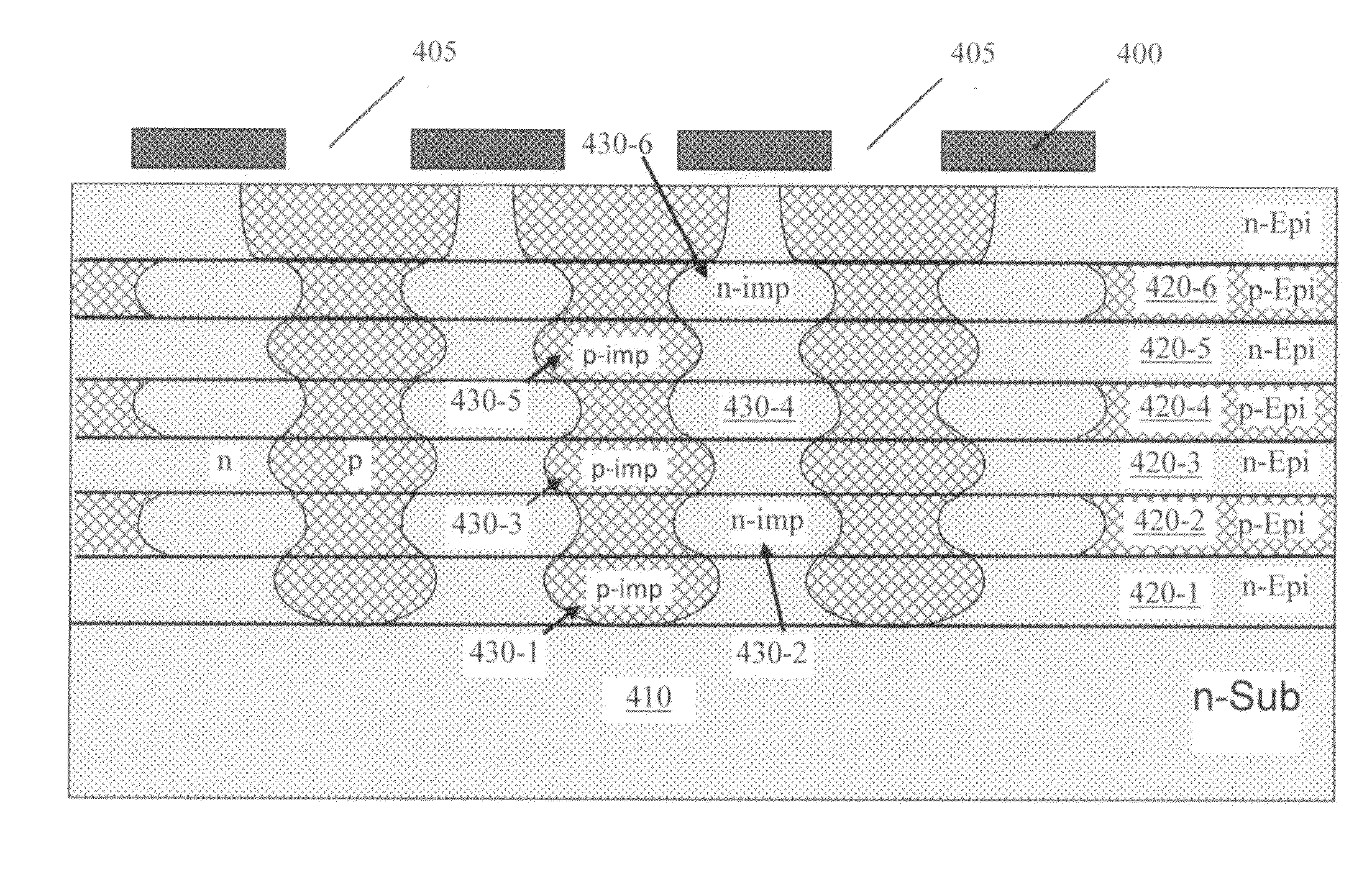
The present invention provides a new and improved manufacturing method to form doped columns in semiconductor devices with alternating conductivity types for charge balance. By simultaneously defining P- and N-implant windows, this method reduces variations in charges in the doped regions and improves the accuracy of the critical dimension. By repeatedly growing and implanting P- and N-doped regions, the variations in column alignment are reduced and the critical dimension of the doped columns can be more strictly controlled, resulting in reduced variation of total charges. This method effectively prevents the adverse effects of critical dimension imbalance that leads to charge imbalance.

Problems solved by technology

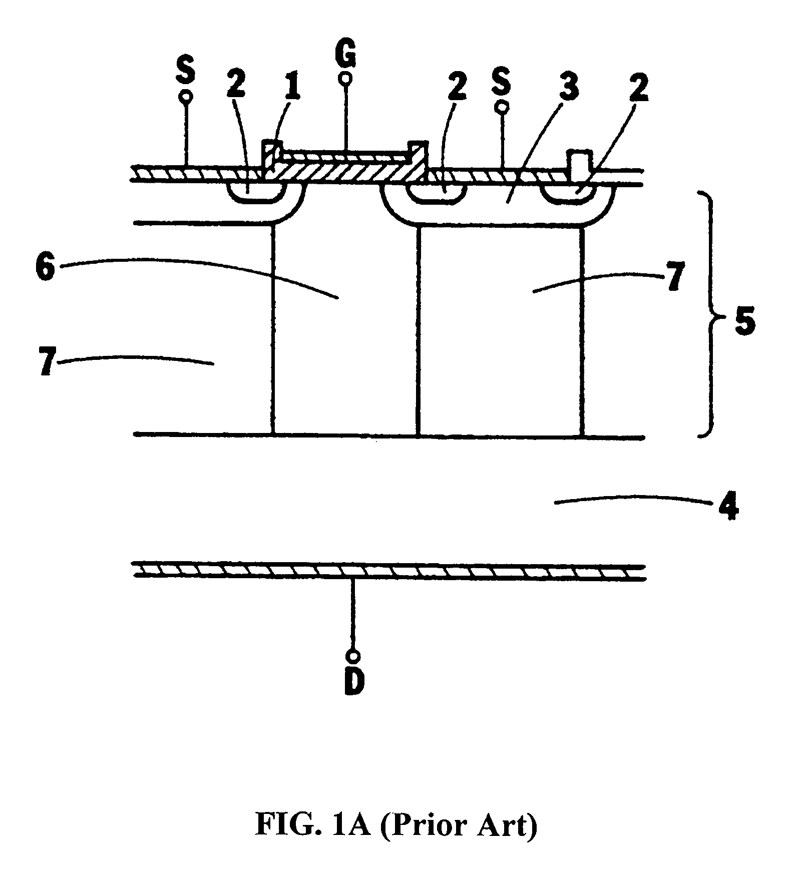
Conventional manufacturing technologies and device configuration to further increase the breakdown voltage with reduced series resistance with a super-junction configuration are still confronted with difficulties and limitations of manufacturability.
The practical applications and usefulness of the high voltage semiconductor power devices are limited due to the facts that the conventional high power devices manufactured with super-junction structural features now encounter difficulties to satisfy the more stringent processing windows.
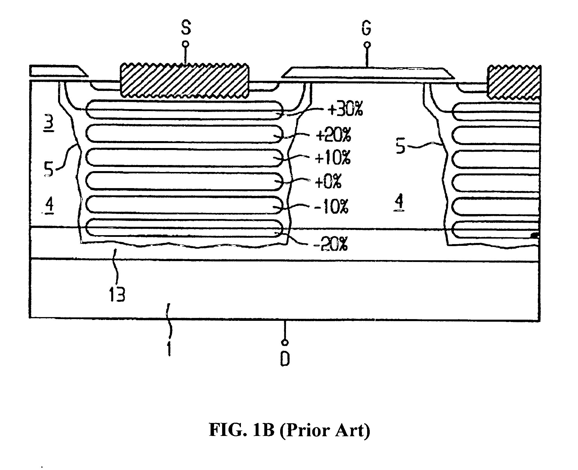
However, the conventional techniques cannot achieve such requirements due to the variation of the N charge for doping the epitaxial layer.
The performance of the super-junction is adversary affected due to the uncontrollable variations of the N charge in the epitaxial layer cannot be further reduced.
However, the variations of charges between the P-doped regions and the N-doped regions in the super-junction structure are significantly beyond the device requirements as now used in the device for more modern applications.
The disclosures of Chen therefore cannot satisfy the more stringent device requirements as now imposed on such devices.
Such dopant variations, even with compensations as disclosed would still not be satisfactory to meet the requirements of current applications with more stringent design windows.

Method used


Image

  • Manufacturing methods for accurately aligned and self-balanced superjunction devices
  • Manufacturing methods for accurately aligned and self-balanced superjunction devices
  • Manufacturing methods for accurately aligned and self-balanced superjunction devices

Examples


Embodiment Construction

[0022]Referring to FIGS. 2A to 2K for a series of cross sectional views for illustrating the processing steps to manufacture a superjunction structure for supporting a semiconductor power device. As shown in FIG. 2A, the manufacturing processes starts from forming an undoped epitaxial layer 110-1 on a heavily doped silicon substrate 105, for example an N-type substrate, followed by forming a hard mask layer 115 and a photoresist coat layer 117 on top of the epitaxial layer 110-1 (FIG. 2B). In FIG. 2C, the photoresist layer 117 is patterned by a mask and the hard mask layer 115 is exposed followed by carrying out a photolithographic etching process to pattern the hard mask layer 115 to form a plurality of implant windows 115′ (FIG. 2D). FIG. 2E-1 shows a first manufacturing approach using only the hard mask by carrying out a N-type ions implant, e.g., phosphorus implant, to form a plurality of N doped regions 120-1 in the epitaxial layer 110-1 followed by applying a P-implant mask 11...


PUM


Abstract

A method for manufacturing a semiconductor power device on a semiconductor substrate supporting a drift region composed of an epitaxial layer by growing a first epitaxial layer followed by forming a first hard mask layer on top of the epitaxial layer; applying a first implant mask to open a plurality of implant windows and applying a second implant mask for blocking some of the implant windows to implant a plurality of dopant regions of alternating conductivity types adjacent to each other in the first epitaxial layer; repeating the first step and the second step by applying the same first and second implant masks to form a plurality of epitaxial layers then carrying out a device manufacturing process on a top side of the epitaxial layer with a diffusion process to merge the dopant regions of the alternating conductivity types as doped columns in the epitaxial layers.

Description

BACKGROUND OF THE INVENTION[0001]1. Field of the Invention[0002]The invention relates generally to the vertical semiconductor power devices. More particularly, this invention relates to configurations and methods with improved manufacturability for manufacturing vertical semiconductor power devices with a super-junction structure for high voltage applications.[0003]2. Description of the Prior Art[0004]Conventional manufacturing technologies and device configuration to further increase the breakdown voltage with reduced series resistance with a super-junction configuration are still confronted with difficulties and limitations of manufacturability. The practical applications and usefulness of the high voltage semiconductor power devices are limited due to the facts that the conventional high power devices manufactured with super-junction structural features now encounter difficulties to satisfy the more stringent processing windows. Specifically, when the target RdsA is reduced from ...

Claims


Application Information

Patent Timeline
Patent Type & Authority Patents(United States)
IPC IPC(8): H01L29/06
CPCH01L29/0634H01L29/1095H01L29/66712H01L29/7802
Inventor GUAN, LINGPENGBOBDE, MADHURBHALLA, ANUPLEE, YEEHENGCHEN, JOHNHO, MOSES
Owner ALPHA & OMEGA SEMICON INC
Learn More