Solid-state image sensing device and semiconductor display device

a sensing device and semiconductor technology, applied in the direction of diodes, semiconductor devices, radio-controlled devices, etc., can solve the problems of narrow detection range, uneven distribution of detectable area, and difficulty in obtaining the positional data of objects at some parts of the pixel portion, so as to reduce uneven distribution of detectable area, and increase the effect of detectable area

Active Publication Date: 2014-08-12
SEMICON ENERGY LAB CO LTD
View PDF122 Cites 8 Cited by
  • Summary
  • Abstract
  • Description
  • Claims
  • Application Information

AI Technical Summary

Benefits of technology

[0009]In view of the above problems, an object of one embodiment of the present invention is to provide a solid-state image sensing device or a semiconductor display device which can easily obtain the positional data of an object without contact. Another object of one embodiment of the present invention is to provide a driving method of a solid-state image sensing device or a semiconductor display device which can easily obtain the positional data of an object without contact.
[0014]Note that besides the above structure, there may be a feature that the first incident angle of light incident on the first photosensor on the upstream of the first incident direction is larger than that of light incident on the first photosensor on the downstream of the first incident direction, when comparing the first incident angles of at least two of the first photosensors, which are different from each other. With such a structure, unevenness of distribution of the detectable area can be reduced and the detectable area can be increased.
[0015]Alternatively, besides the above structure, there may be a feature that the second incident angle of light incident on the second photosensor on the upstream of the second incident direction is larger than that of light incident on the second photosensor on the downstream of the second incident direction, when comparing the second incident angles of at least two of the second photosensors, which are different from each other. With such a structure, unevenness of distribution in the detectable area can be reduced and the detectable area can be increased.
[0016]According to one embodiment of the present invention, a solid-state image sensing device or a semiconductor display device, which can easily obtain the positional data of an object without contact, can be provided. According to another embodiment of the present invention, a driving method of a solid-state image sensing device or a semiconductor display device, which can easily obtain the positional data of an object without contact, can be provided.

Problems solved by technology

However, in the case of the touchscreen disclosed in Non-Patent Document 1, a detectable area where light from an object can be detected is narrow and distribution of the detectable area is uneven.
In the case where the detectable area is narrow and distribution of the detectable area is uneven, it becomes difficult to obtain the positional data of an object at some parts of the pixel portion even when the object is only slightly distant from a surface of the touchscreen.
Thus, when a finger, a stylus, or the like is brought closer to the touchscreen, positional data can be obtained in some cases and cannot be obtained in other cases depending on a part of the pixel portion, which is inconvenient for a user.
Further, it is necessary to directly touch the surface of the touchscreen in order to obtain positional data in some cases depending on a part of the pixel portion, resulting in deterioration in quality of the touchscreen according to the use frequency; for example, the surface of the touchscreen might get dirty or have a scratch mark.
Moreover, a finger directly touches the surface of the touchscreen repeatedly, so that fatigue of a user might be increased.
However, when the range of an incident angle of light incident on each photosensor is simply widen to expand a detectable area, light with low directivity is received by the photosensor.
Consequently, the detected position of an object and the actual position of the object are misaligned; thus, accuracy of the positional data is lowered.

Method used


Image

  • Solid-state image sensing device and semiconductor display device
  • Solid-state image sensing device and semiconductor display device
  • Solid-state image sensing device and semiconductor display device

Examples


embodiment 1

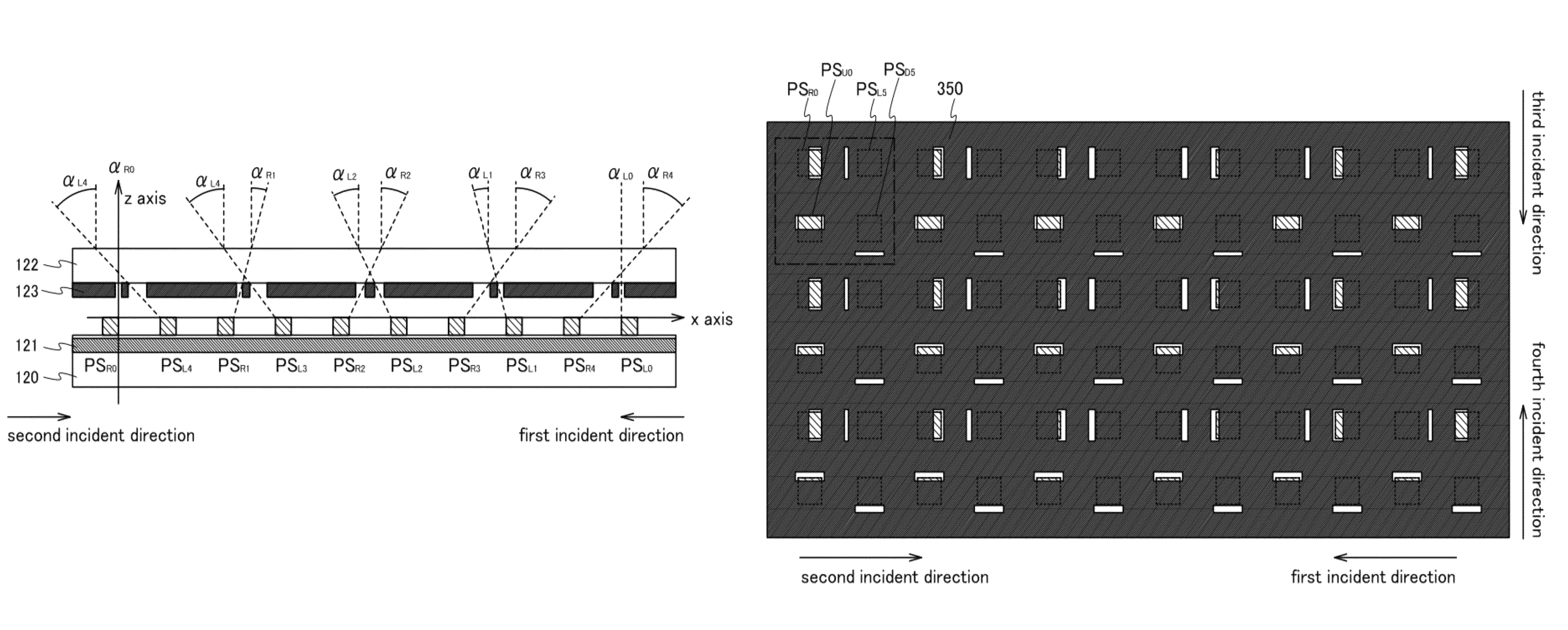
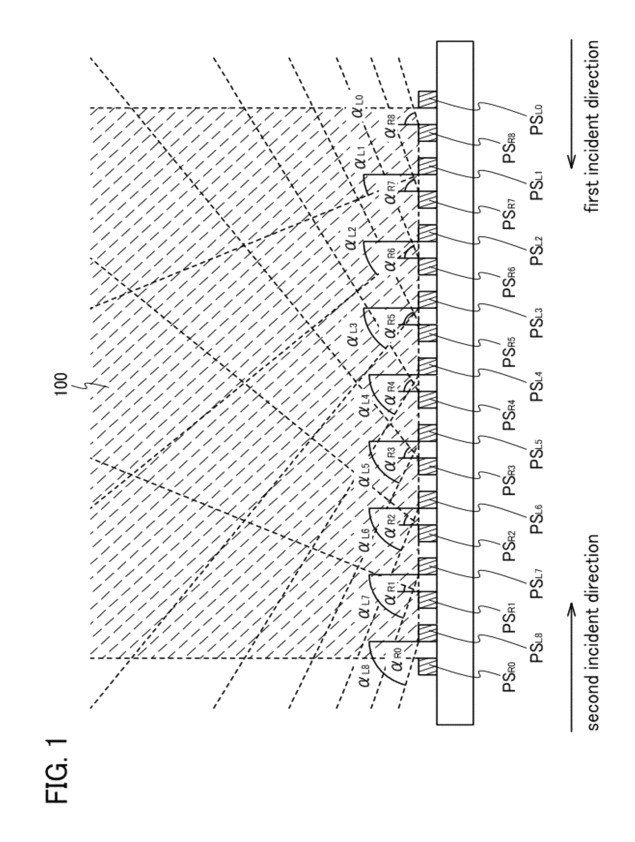
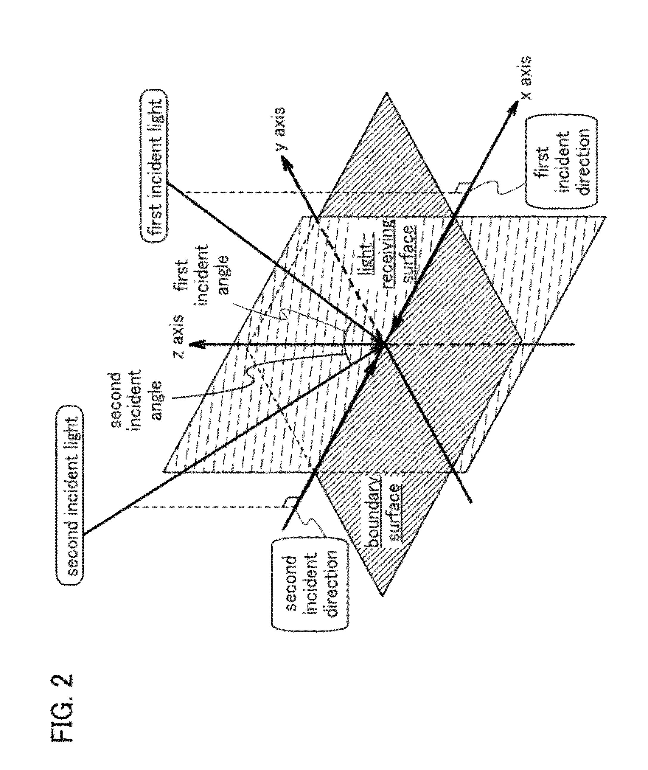
[0062]A solid-state image sensing device or a semiconductor display device, according to one embodiment of the present invention, includes a plurality of photosensors in a pixel portion. The plurality of photosensors can be classified by the incident direction of incident light. A solid-state image sensing device or a semiconductor display device, according to one embodiment of the present invention, includes at least a plurality of first photosensors and a plurality of second photosensors. Light from a first incident direction enters the plurality of first photosensors. Light from a second incident direction different from the first incident direction enters the plurality of second photosensors.

[0063]A solid-state image sensing device or a semiconductor display device, according to one embodiment of the present invention, will be described taking a structure of a pixel portion where a plurality of first photosensors PSR's and a plurality of second photosensors PSL's are alternately...

embodiment 2

[0117]In this embodiment, a specific structure of a photosensor included in a solid-state image sensing device or a semiconductor display device, according to one embodiment of the present invention, will be described.

[0118]FIG. 7A is an example of a circuit diagram illustrating a connection configuration of a photosensor 301. The photosensor 301 includes a photodiode 302 and an amplifier circuit 303. The photodiode 302 is a photoelectric conversion element which generates current when a junction of semiconductors is exposed to light. The amplifier circuit 303 is a circuit which amplifies current obtained through light reception by the photodiode 302 or a circuit which holds electric charge accumulated with the current.

[0119]The configuration of the amplifier circuit 303 may be any configuration as long as current generated in the photodiode 302 can be amplified or electric charge accumulated with the current can be held. It is necessary that the amplifier circuit 303 include a tran...

embodiment 3

[0226]In this embodiment, the photosensor 301 having a circuit configuration different from that in FIG. 7A will be described.

[0227]FIG. 20A is a circuit diagram of an example of the photosensor 301. In the photosensor 301 illustrated in FIG. 20A, the amplifier circuit 303 includes a transistor 304, a transistor 305, a transistor 306, and a transistor 307. The transistor 304 controls the supply of current generated in the photodiode 302 to the amplifier circuit 303. In the transistor 305, the current value or resistance value between a first terminal and a second terminal thereof depends on a potential supplied to the second terminal of the transistor 304. The transistor 306 functions as a switching element for supplying a potential of an output signal determined by the current value or resistance value, to the wiring OUT. The transistor 307 functions to reset the amount of electric charge accumulated in the amplifier circuit 303.

[0228]Specifically, in FIG. 20A, a first terminal of ...


PUM


Abstract

To provide a solid-state image sensing device or a semiconductor display device, which can easily obtain the positional data of an object without contact. Included are a plurality of first photosensors on which light with a first incident angle is incident from a first incident direction and a plurality of second photosensors on which light with a second incident angle is incident from a second incident direction. The first incident angle of light incident on one of the plurality of first photosensors is larger than that of light incident on one of the other first photosensors. The second incident angle of light incident on one of the plurality of second photosensors is larger than that of light incident on one of the other second photosensors.

Description

BACKGROUND OF THE INVENTION[0001]1. Field of the Invention[0002]The present invention relates to a solid-state image sensing device including a photosensor in a pixel, and to a semiconductor display device including a photosensor and a display element in a pixel.[0003]2. Description of the Related Art[0004]A photosensor utilizing an amplifying function of a MOS transistor, called a CMOS sensor, can be manufactured through a general CMOS process. Thus, a solid-state image sensing device including a CMOS sensor can be manufactured at lower cost than a solid-state image sensing device including a CCD sensor. A CMOS sensor and a display element are formed over one substrate, whereby a semiconductor display device having both a function of an input device and a function of a display device, called a touchscreen, can be fabricated.[0005]In recent years, a technique of taking three-dimensional images of an object has been increasingly demanded with an expansion of the markets of three-dime...

Claims


Application Information

Patent Timeline
Patent Type & Authority Patents(United States)
IPC IPC(8): H01L27/15
CPCH01L27/14687H01L27/1469H01L27/14634H01L27/14632H01L27/14643H01L27/1443H01L27/1464H01L27/14623
Inventor KUROKAWA, YOSHIYUKIIKEDA, TAKAYUKI
Owner SEMICON ENERGY LAB CO LTD
Why Eureka
Try Eureka