System and method for transfer of data between memory with dynamic error recovery

a technology of dynamic error recovery and data transfer, which is applied in the field of system and method for transferring data between memory with dynamic error recovery, can solve the problems of dramatically reducing the size, affecting the reliability of designed circuits (and particularly memory modules incorporating such transistors), and affecting the reliability of data transfer. , to achieve the effect of reliable data transfer

Active Publication Date: 2014-08-19
CADENCE DESIGN SYST INC
View PDF11 Cites 23 Cited by
  • Summary
  • Abstract
  • Description
  • Claims
  • Application Information

AI Technical Summary

Benefits of technology

[0017]A system realized in accordance with the present invention includes ensuring reliable data transfer by automatically recovering from un-correctable errors during transfers from a first memory to a second memory via a storage intermediary. A transfer controller is coupled to and transfers data packets between a first memory and a second memory. A storage intermediary is disposed intermediate the first and second memories. The storage intermediary temporarily stores data packets destined for the second memory. An error detection module signals the transfer controller to retrieve a replacement data portion of a corrupt data packet from the first memory responsive to an affirmative determination of corruption in a data packet retrieved from the storage intermediary. A bypass controller is coupled intermediate to the first memory and the second memory, the bypass controller selectively transmits the replacement data portion to the second memory. The transmitting bypasses the storage intermediary r

Problems solved by technology

These errors are particularly likely where the second memory is generally slower and requires a rate-matching buffer or temporary storage interface between the first and second memories.
During the course of data transfer between memory devices, the transferred data may be corrupted by errors deriving from various sources.
As circuit design progresses, dies shrink, the size of component features (most notably transistors) therein dramatically decrease in size, the designed circuits (and particularly memory modules incorporating such transistors) become less reliable.
As the dies and fabrication processes create smaller and smaller features, such as the progression from, for example 90 nanometer feature size to 65 nm, 45 nm, 32 nm, 22 nm and beyond, the individual transistors and other features of the circuit become more susceptible to quantum phenomena such as cell leakage or charge migration, amongst other problems.
In such an event, the charge may undesirably migrate through insulative dielectric layers resulting in unknown unintended system states, leading perhaps to catastrophic system failure.
Increasing clock rates, low power constraints, and unfavorable environments, only exacerbate such issues.
These phenomena have a measurable and significant negative impact on system memory, busses, processors, and other components.
Aside from quantum phenomena, all manner of issues may act to degrade system performance and result in errors at virtually any stage of a system such as, for example, transmission line errors, interference, crosstalk, parasitic capacitance, power surges, spikes, and the like.
As distances between traces in a routed circuit become smaller and densities increase, such parasitics and resultant errors in transmission, storage, and reception become increasingly more likely.
Indeed, errors may occur in countless manners throughout virtually any components and/or interconnects throughout a system.
One such example of error-prone components are transistors within a densely packed circuit design.
Charge stored in transistors or devices such as flip flops may represent mission-critical data, and if the charge is lost through cell migration or other such quantum phenomena, the mission-critical data may

Method used


Image

  • System and method for transfer of data between memory with dynamic error recovery
  • System and method for transfer of data between memory with dynamic error recovery
  • System and method for transfer of data between memory with dynamic error recovery

Examples


Embodiment Construction

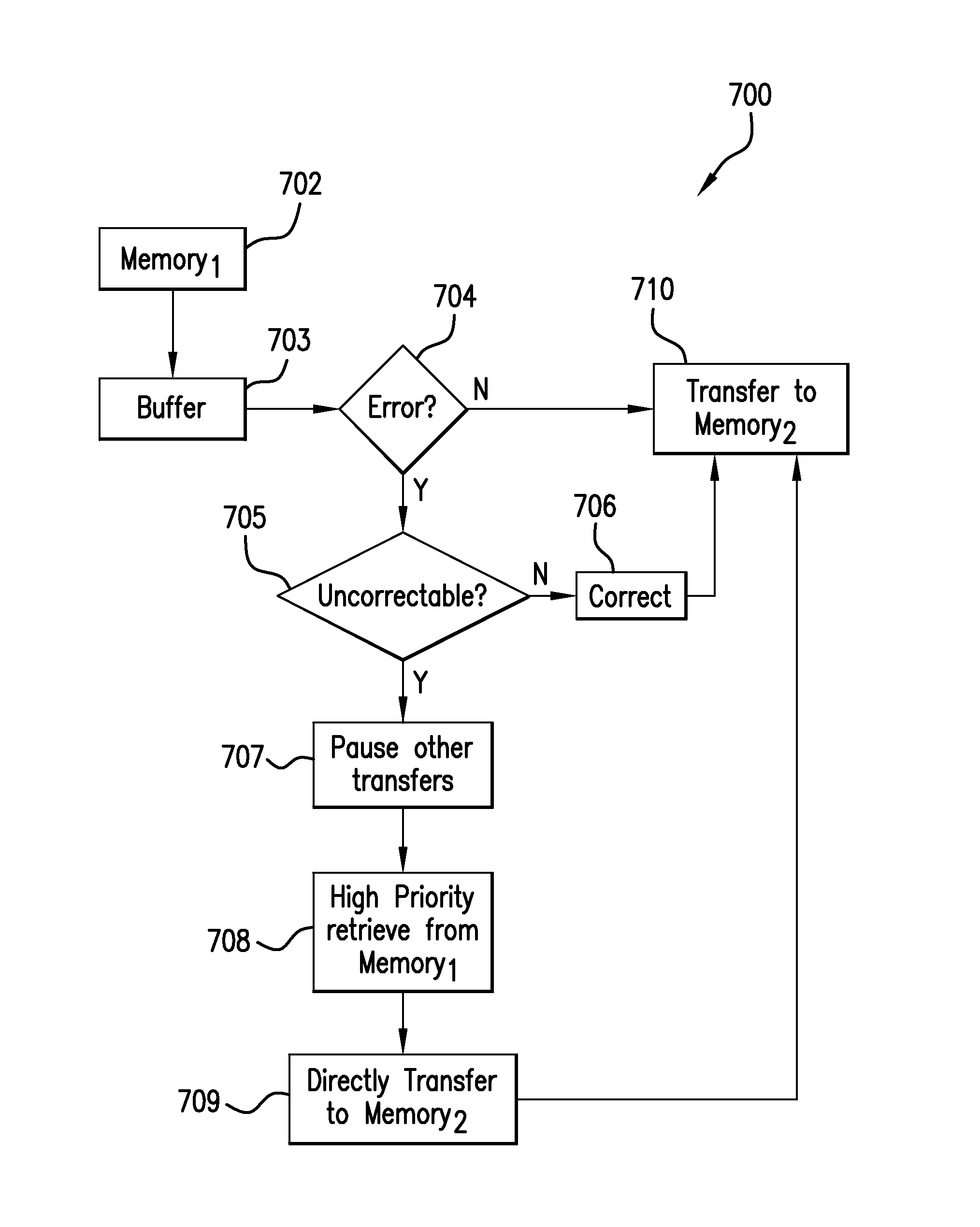
[0030]One example of the system and method realized in accordance with the disclosed embodiment seeks to provide and ensure reliable transfer of data from one memory to another memory and provide for automated recovery from an uncorrectable error encountered in a transfer from the first memory to the second memory by way of an unreliable intermediate buffer. Another example of the system and method realized in accordance with the present invention seeks to mitigate the dangers of an unreliable buffer memory such as SRAM.

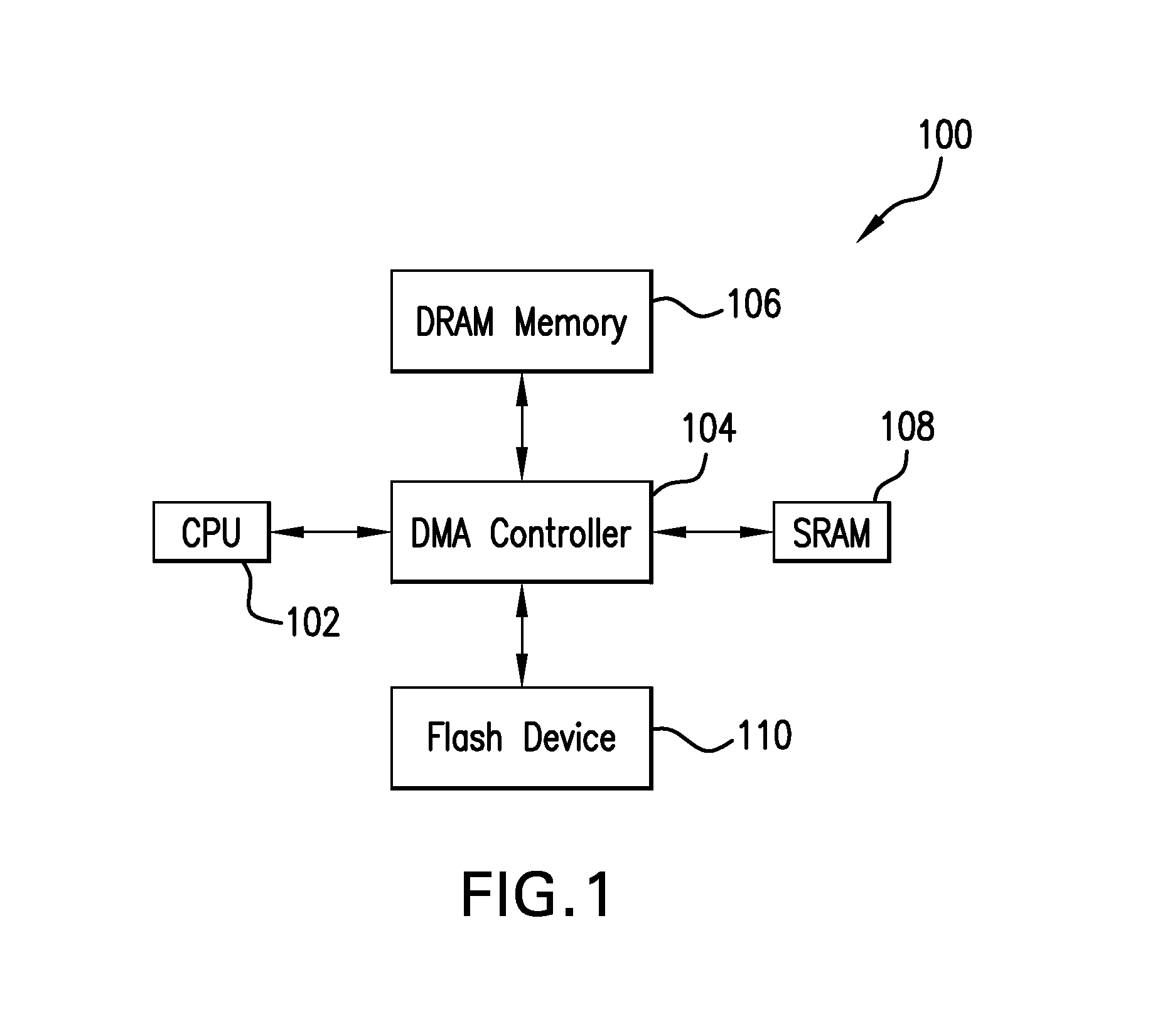
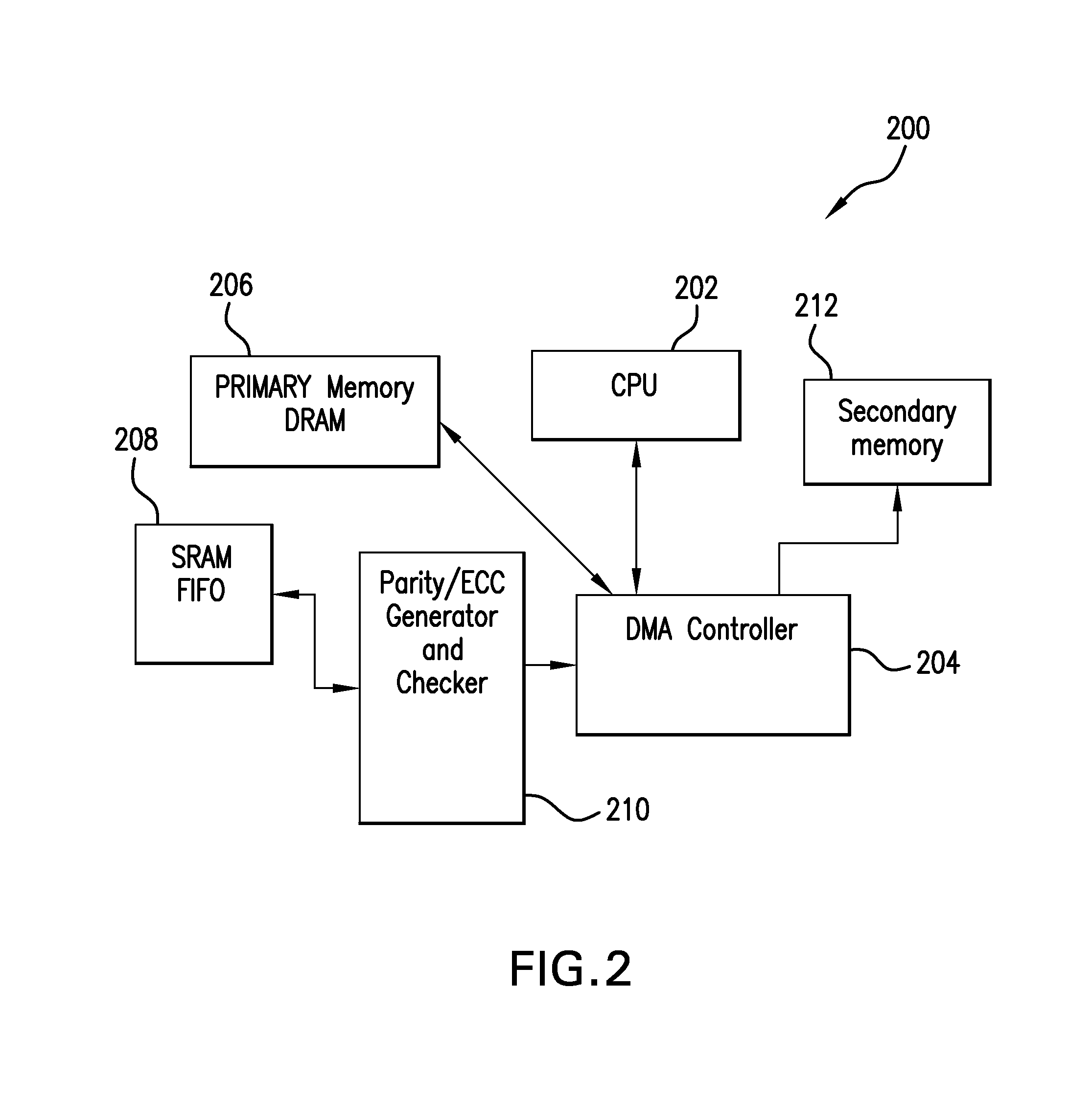
[0031]As seen in the illustrative diagram of FIG. 1, a system 100 includes a central processing unit (CPU) 102 intercoupled with a direct memory access (DMA) controller 104 itself coupled to a first memory 106 (referred to herein illustratively as a DRAM memory), a secondary memory 110 (referred to illustratively throughout as a flash device), and a buffer 108 (illustratively referred to herein as an SRAM FIFO). First memory 106 is preferably a DRAM or dynamic random...


PUM


Abstract

A system and method are provided for ensuring reliable data transfers by automatically recovering from un-correctable errors detected in data traversing throughout a system and being retrieved from an unreliable intermediate data buffer between a first memory and a secondary slower memory. Additionally, measures to compensate for the use of unreliable or error-prone components and interconnects, such as, for example, SRAM memory as a temporary buffer are provided. Further, measures to detect and correct errors—whatever the type—injected or occurring at any stage throughout traversal of the system are provided.

Description

[0001]The subject system and method are generally directed to ensuring reliable and accurate transfer of data throughout a system, and particularly, from a first memory to a second memory by way of at least one intermediate location with mid-stream error detection and remediation. Additionally, self-recovery from uncorrectable system errors and failures during a data transfer throughout a system is provided. These errors are particularly likely where the second memory is generally slower and requires a rate-matching buffer or temporary storage interface between the first and second memories. The system and method provide automated measures for preventing system failure and responding seamlessly to uncorrectable errors detected mid-stream in a data segment retrieved from an intermediate location such as, for example, a static ram (SRAM) buffer during a transfer of a requested frame of data. During the course of data transfer between memory devices, the transferred data may be corrupt...

Claims


Application Information

Patent Timeline
IPC IPC(8): G06F11/00
CPCG06F11/00G06F11/1443G06F11/10G06F13/00G06F13/28
Inventor LAHON, MANASBRAHMADATHAN, SANDEEP
Owner CADENCE DESIGN SYST INC
Why Eureka
Try Eureka