Method of manufacturing semiconductor device, method of processing substrate, substrate processing apparatus and non-transitory computer-readable recording medium

a semiconductor and processing method technology, applied in the direction of coatings, chemical vapor deposition coatings, metallic material coating processes, etc., can solve the problems of complex control of the three kinds of gases, inability to achieve a high concentration of 25 at % or more, and reduce the productivity of film formation in some cases. , to achieve the effect of increasing the carbon concentration in the carbonitride film and improving productivity

Active Publication Date: 2014-08-26
KOKUSA ELECTRIC CO LTD +1
View PDF12 Cites 4 Cited by
  • Summary
  • Abstract
  • Description
  • Claims
  • Application Information

AI Technical Summary

Benefits of technology

[0021]According to the present invention, there is provided a method of manufacturing a semiconductor device, a method of processing a substrate, a substrate processing apparatus and a non-transitory computer-readable recording medium, capable of improving productivity during film formation of a carbonitride film, and increasing a carbon concentration in the carbonitride film.

Problems solved by technology

However, control of the three kinds of gases is complicated, and when the above-mentioned technique is used, productivity during film formation is reduced in some cases.
In addition, when the above-mentioned technique is used, it is not easy to obtain a high concentration of 25 at % or more for example, regarding a carbon concentration in the silicon carbonitride film.

Method used


Image

  • Method of manufacturing semiconductor device, method of processing substrate, substrate processing apparatus and non-transitory computer-readable recording medium
  • Method of manufacturing semiconductor device, method of processing substrate, substrate processing apparatus and non-transitory computer-readable recording medium
  • Method of manufacturing semiconductor device, method of processing substrate, substrate processing apparatus and non-transitory computer-readable recording medium

Examples


example

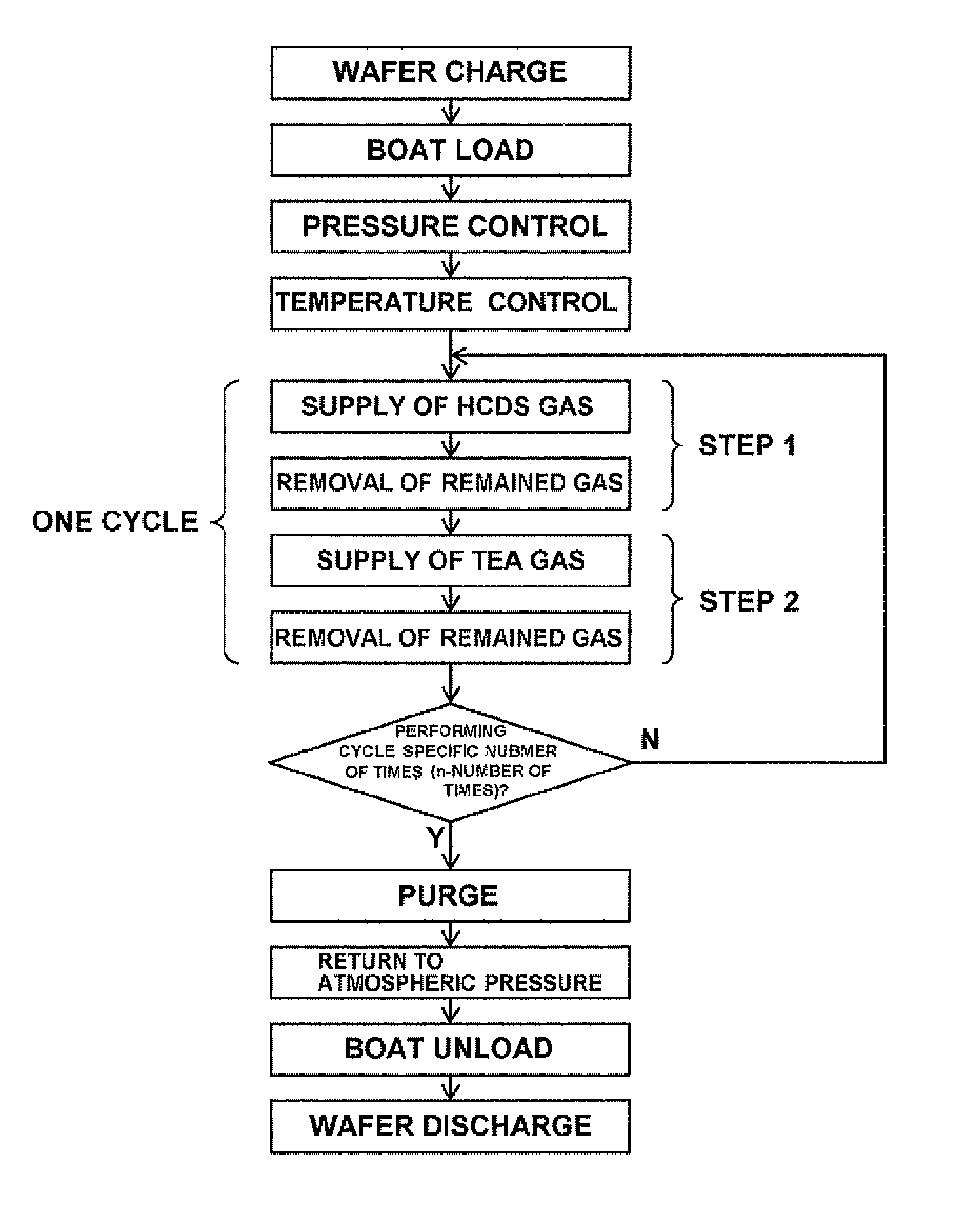
[0141]The SiCN film was formed on a plurality of wafers in the above-mentioned sequence, using the substrate processing apparatus of the above-mentioned embodiment. The HCDS gas was used as the source gas, and the TEA gas was used as the reactive gas. A wafer temperature during film formation was set to 600 to 650° C. Other processing condition was set to a specific value within a range of the processing condition of the above-mentioned embodiment. Then, the uniformity in the film thickness of the formed SiCN film in-plane of the wafer (called WTW, hereafter), the uniformity in film thickness of the formed SiCN films inter-planes of the wafers (called WTW, hereafter), a refractive index (called R.1., hereafter), a XPS composition ratio, and a wet etching rate with respect to a hydrogen fluoride (HF)-containing liquid (called WER, hereafter) having a concentration of 1.0%, were respectively measured. Measurement results thereof are shown in FIG. 7.

[0142]As shown in FIG. 7, it was con...


PUM

PropertyMeasurementUnit
pressureaaaaaaaaaa
pressureaaaaaaaaaa
pressureaaaaaaaaaa

Abstract

There is provided a method of manufacturing a semiconductor device, including: forming a film containing a specific element, nitrogen, and carbon on a substrate, by alternately performing the following steps a specific number of times: a step of supplying a source gas containing the specific element and a halogen element, to the substrate; and a step of supplying a reactive gas composed of three elements of carbon, nitrogen, and hydrogen and having more number of a carbon atom than the number of a nitrogen atom in a composition formula thereof, to the substrate.

Description

TECHNICAL FIELD[0001]The present invention relates to a method of manufacturing a semiconductor device including a step of forming a thin film on a substrate, a method of processing a substrate, a substrate processing apparatus and a non-transitory computer-readable recording medium.DESCRIPTION OF RELATED ART[0002]Manufacturing steps of a semiconductor device include a step of forming a silicon-based insulating film such as a silicon oxide film (a SiO2 film, simply called a SiO film hereafter) and a silicon nitride film (a Si3N4 film, simply called a SiN film hereafter), etc., namely include a step of forming an insulating film containing silicon as a specific element, on a substrate such as a silicon wafer. The silicon oxide film has excellent insulation properties and low dielectric properties, and is widely used as the insulating film and an inter-layer film. The silicon nitride film has excellent insulation properties, corrosion resistance, dielectric properties, and film stress...

Claims


Application Information

Patent Timeline
Patent Type & Authority Patents(United States)
IPC IPC(8): H01L21/31H01L21/02H01L21/318
CPCH01L21/3185H01L21/02211H01L21/02183H01L21/02167H01L21/0228H01L21/02189H01L21/02186H01L21/02181H01L21/02178H01L21/02175C23C16/36C23C16/45553
Inventor HIROSE, YOSHIROSANO, ATSUSHIYANAGITA, KAZUTAKAHIGASHINO, KATSUKO
Owner KOKUSA ELECTRIC CO LTD
Why Eureka
Try Eureka