

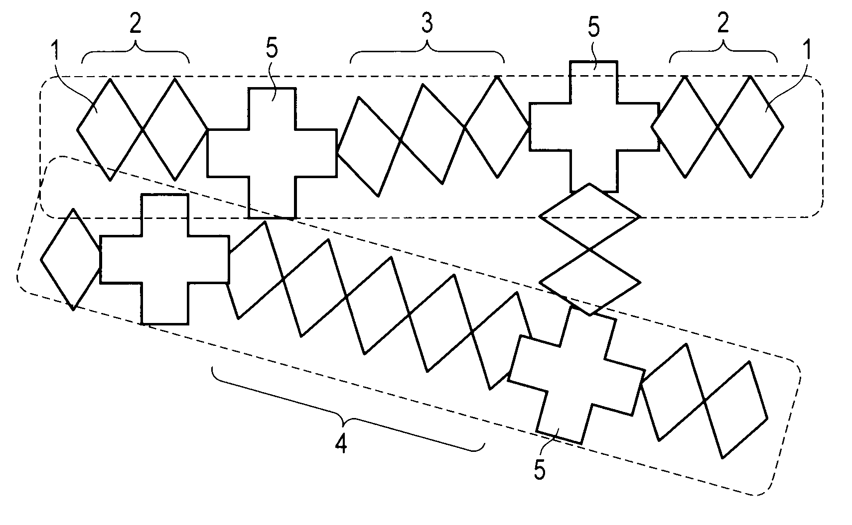
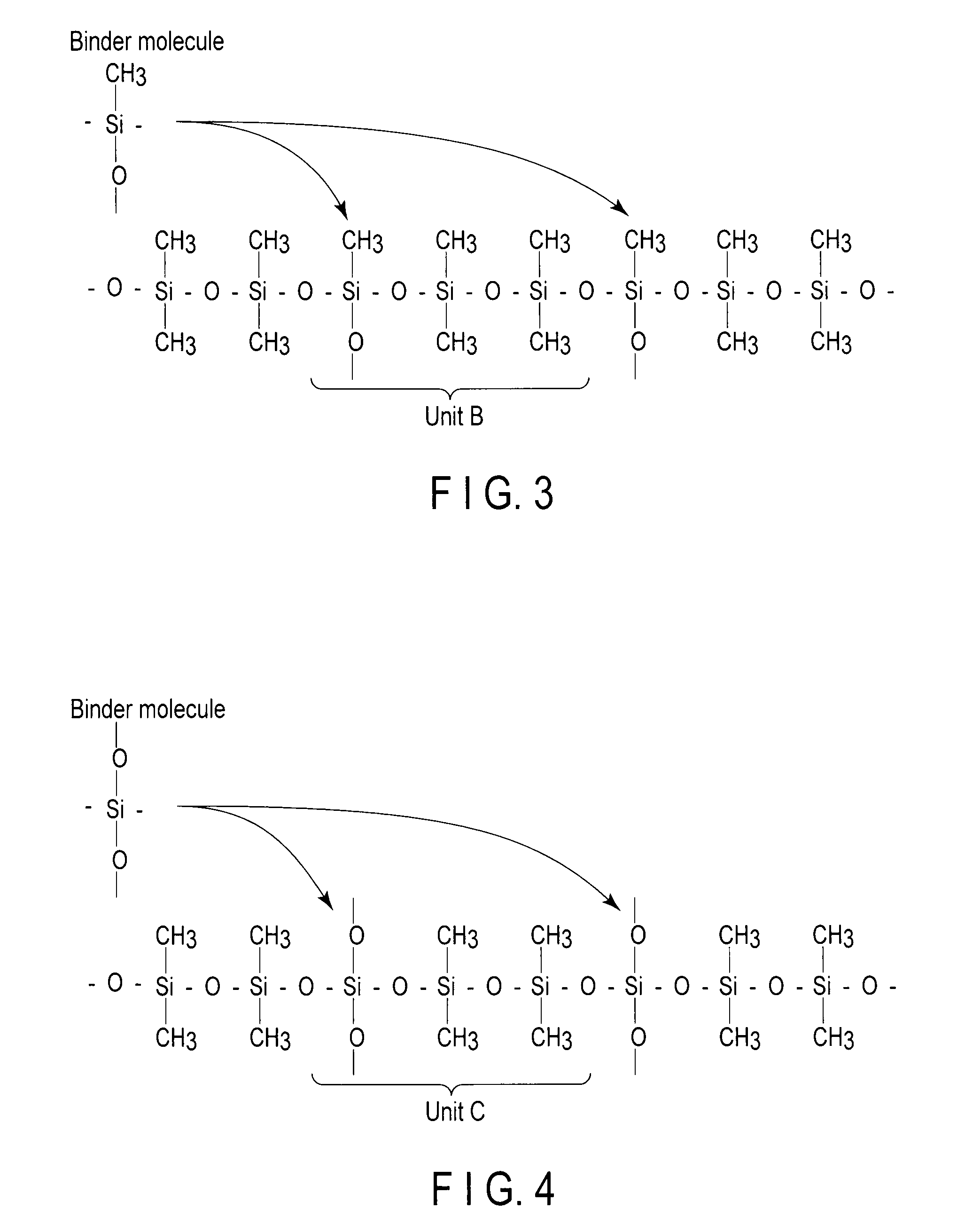
Low dielectric constant insulating film and method for forming the same
a technology of low dielectric constant and insulating film, which is applied in the direction of coating, chemical vapor deposition coating, metallic material coating process, etc., can solve the problems of reducing the concentration of chsub>3 /sub>in the film, the film strength is dropped, and the effect of high mechanical strength
- Summary
- Abstract
- Description
- Claims
- Application Information
AI Technical Summary
Benefits of technology
Problems solved by technology
Method used
Image

Examples
example 1
[0106]Two kinds of insulating films were deposited on silicon substrates, respectively, employing the neutral particle beam irradiation type CVD apparatus shown in FIG. 6 and using DMDMOS and DMOTMDA as a raw gas. Each of the silicon substrates was continuously irradiated with neutral beams having energy of 10 eV. A pressure in a chamber was kept at 30 mTorr, and a temperature of the substrate was −20° C. Incidentally, an insulating film was deposited on a silicon substrate by the conventional plasma CVD (PECVD) using DMOTMDA as a raw gas as a comparative example.
[0107]Thus obtained three insulating films were analyzed by means of a Fourier transform infrared spectroscopy. k values of the insulating films were measured by means of Hg probe, and Young' moduli of the insulating films were measured by means of nanoindentor. These results were shown in the following Table 1.
[0108]
TABLE 1PECVDC-NBE-CVDDMOTMDSDMDMOSDMOTMDSFTIRSiOLinear3752.851.2struc-Network5325.830.5tureCage1021.618.3CH3...
example 2
[0111]An insulating film was deposited on a silicon substrate in the same manner as in Example 1 except that DMOTMDA was used as a raw gas and the substrate was cooled to at a temperature of −70° C. The obtained film was analyzed by a Fourier transform infrared spectroscopy. k value of the insulating films was measured by means of Hg probe, and Young' modulus was measured by means of nanoindentor. These results were shown in the following Table 2. Table 2 showed also data of the insulating film formed by the conventional PECVD method in Example 1 and the insulating film formed by the NBE-CVD method with the substrate being cooled to −20° C.
[0112]
TABLE 2C-NBE-CVDPECVDSubstrate temperatureDMOTMDS−20° C.−70° C.FTIRSiOLinear3751.249.2struc-Network5330.528.2tureCage1018.322.6CH3Si(CH3)2 / 4285.789.2Si(CH3)1+2k value2.61.91.7Young' modulus (GPa)747
[0113]As shown in the above Table 2, the insulating film formed by the NBE-CVD method with the temperature of the substrate being cooled to −70° ...
example 3
[0116]An insulating film was deposited on a silicon substrate in the same manner as in Example 2 except that the substrate was irradiated with neutral beams in a pulsed form. The film was formed in such a condition that pulse-on time was fixed to 50 μs, and pulse-off time was changed. Thus obtained films were analyzed by means of a Fourier transform infrared spectroscopy and change in composition of SiO structure was examined. The results are shown in FIG. 13.
[0117]As shown in FIG. 13, a content of linear structure molecules in the insulating film increases as the pulse-off time increases. In particular, a content of linear structure molecules in the insulating film attains to 52% or more in a pulse-off time of 100-200 μs, and on the other hand, a content of network structure molecules decreases. As a result, k value decreases to 1.3 and Young' modulus of more than 5 GPa is obtained.
PUM
| Property | Measurement | Unit |
|---|---|---|
| wavenumber | aaaaa | aaaaa |
| wavenumber | aaaaa | aaaaa |
| dielectric constant | aaaaa | aaaaa |
Abstract
Description
Claims
Application Information