VIS-NIR plasmonic APD detectors
a plasmonic apd and detector technology, applied in the field ofavalanche photodiodes, can solve the problems of low noise, operating temperature substantially affecting both the noise level and bias voltage point of the geiger
- Summary
- Abstract
- Description
- Claims
- Application Information
AI Technical Summary
Benefits of technology
Problems solved by technology
Method used
Image
Examples
embodiments
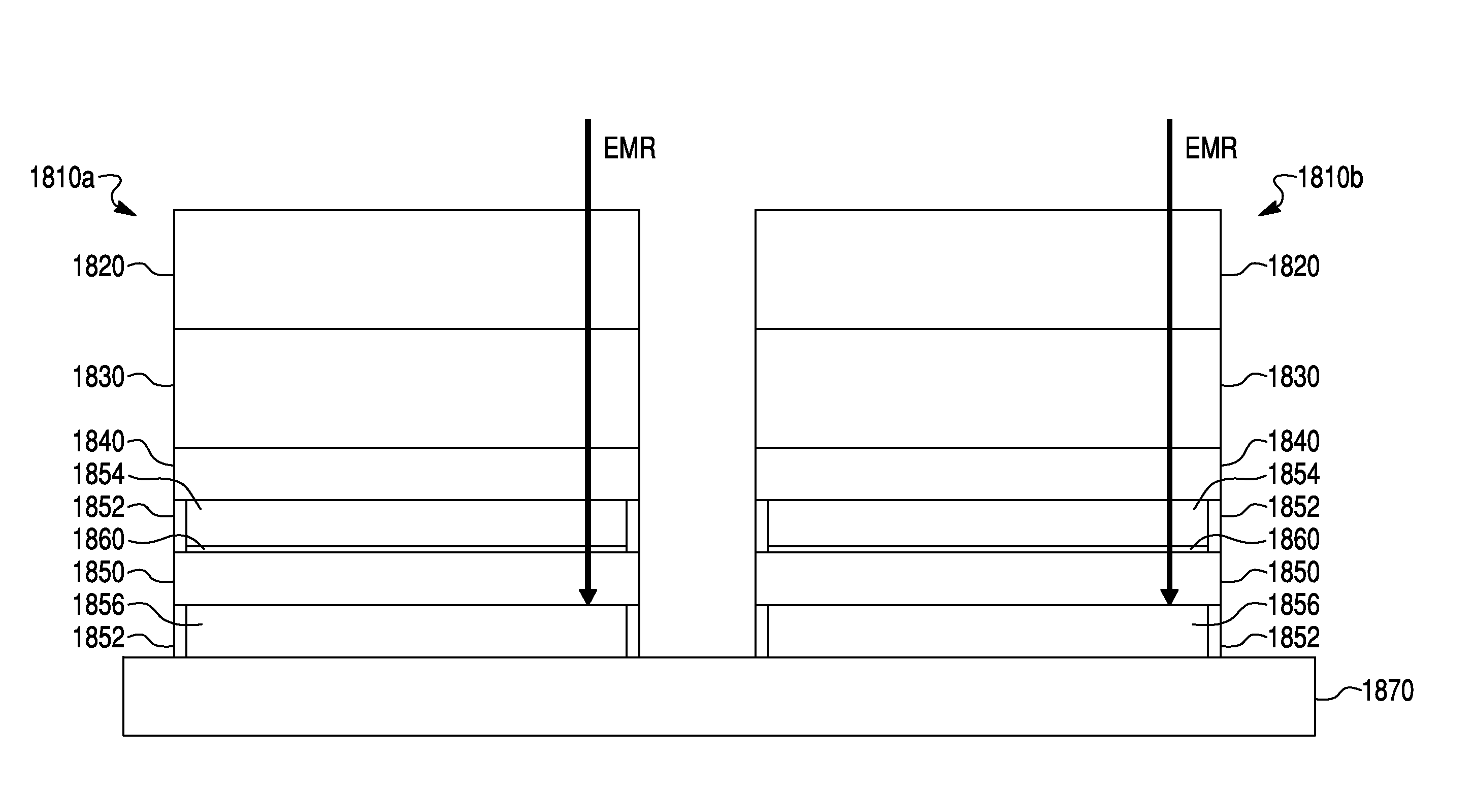
[0058]FIG. 5A illustrates a schematic of an APD EMR detector according to one embodiment. The APD EMR detector includes an EMR absorption region 10, which is the detector material 216, a voltage biasing element 240, and a charge multiplication region 20. The detector material 216 includes a substantially regular array 212 of nanoparticles 210 embedded in a matrix material 214. The voltage biasing element 240 is configured to apply a bias voltage to the matrix material 214 such that electrical current is directly generated based on a cooperative plasmon effect in the detector material when electromagnetic radiation in a predetermined wavelength range is incident upon the detector material, where the dominant mechanism for decay in the cooperative plasmon effect is nonradiative. The charge multiplication region 20 is arranged relative to the EMR absorption region 10 to avalanche multiply the electrical current generated in the EMR absorption region 10.
[0059]The nanoparticles 210 may c...
PUM
 Abstract
Description
Claims
Application Information


