

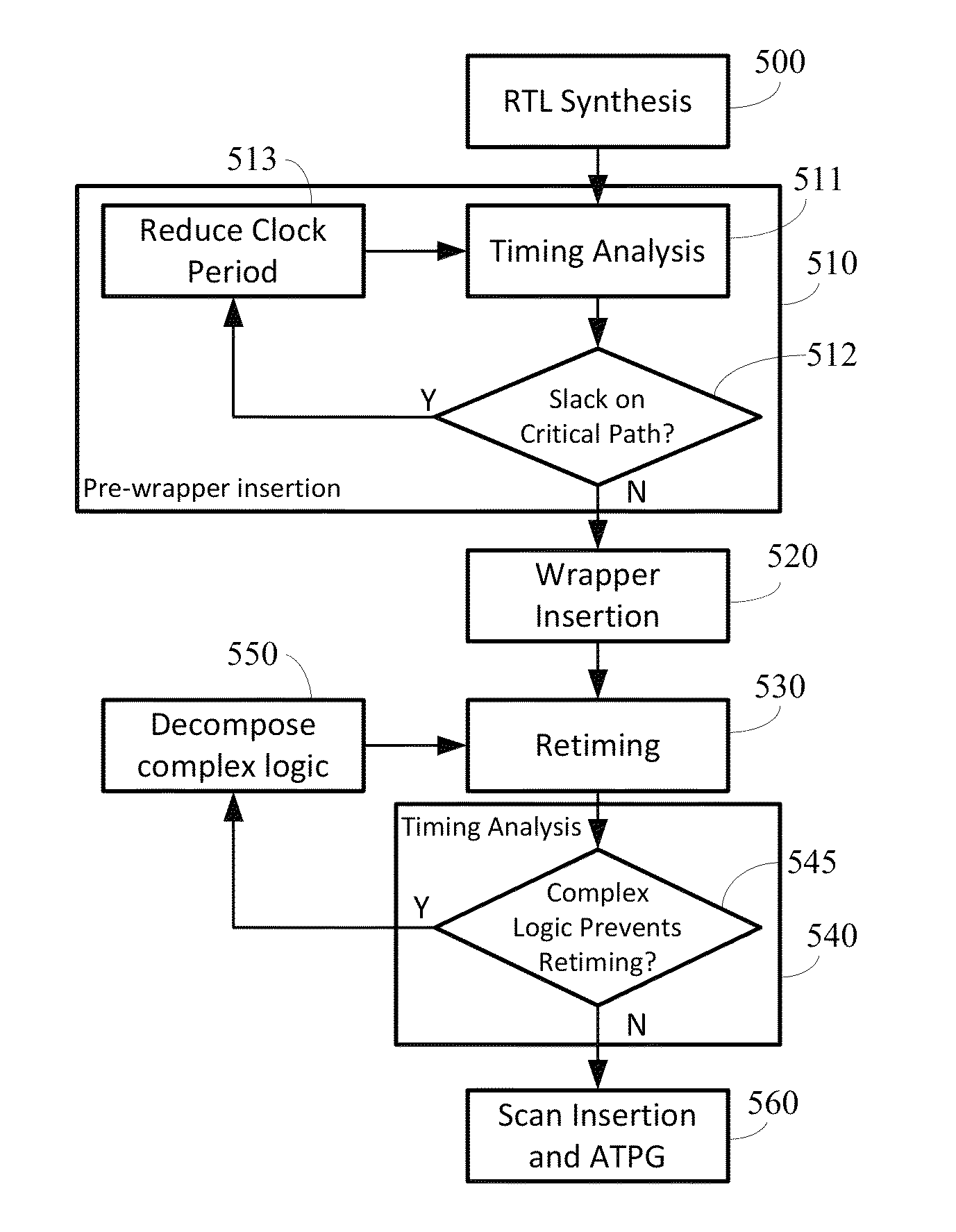
Retiming-based design flow for delay recovery on inter-die paths in 3D ICs
a design flow and interdie path technology, applied in the field of retiming-based design flow for delay recovery on interdie path in 3d ics, can solve the problems of increasing load and delay, affecting the functional timing or latency of interdie path, interconnect delay becoming a significant contributor to circuit latency, etc., and achieve the effect of improving latency
- Summary
- Abstract
- Description
- Claims
- Application Information
AI Technical Summary
Benefits of technology
Problems solved by technology
Method used
Image

Examples
example —
Example—Simulation Results
[0075]For the example simulations, the retiming algorithm used to apply to the circuits is from Synopsys Design Compiler, which performs retiming first to minimize clock period and then to minimize register count. This is followed by a combinational logic optimization step in view of changes to loading on cells and critical paths that may have occurred after the movement of registers.
[0076]The effectiveness and impact of post-DfT-insertion retiming on a benchmark circuit that has been partitioned into two-, three-, and four-die stacks was examined. A number of OpenCore benchmarks, obtained from an open source project originating from OpenCores.org, were used.
[0077]To show retiming, the performance-optimized data encryption standard (DES) circuit and the Fast Fourier Transform (FFT) circuit from the IWLS 2005 OpenCore benchmarks were used. The DES circuit contains 26,000 gates and 2,000 flops, while the FFT circuit contains 299,273 gates with 19,962 flops. T...
PUM
 Abstract
Description
Claims
Application Information