Compound-barrier infrared photodetector

a technology of infrared photodetector and compound barrier, which is applied in the direction of solid-state devices, semiconductor devices, radio-controlled devices, etc., can solve the problems of variations in electric field in the narrow-bandgap absorber region of the detector structure, and the failure to provide mechanisms to minimize the effects of surface recombination/generation in the periphery

Active Publication Date: 2014-09-16
HRL LAB
View PDF13 Cites 23 Cited by
  • Summary
  • Abstract
  • Description
  • Claims
  • Application Information

AI Technical Summary

Benefits of technology

[0012]In an alternative embodiment, a compound barrier infrared photodetector comprising: an absorber layer responsive to infrared light, a first barrier layer disposed on the absorber layer, a second barrier layer disposed on the first barrier layer, a contact layer disposed on the second barrier layer in a first region, wherein the first barrier layer and the second barrier layer are each selected to allow minority carrier transport both outside and inside the first region. The minority carrier transport outside the first region is substantially blocked when a reasonable bias voltage is applied to the contact layer relative to the absorber layer. Moreover, the first barrier layer comprises a III-V semiconductor alloy selected from the AlGaInPAsSb family of semiconducting alloys. In addition, the first barrier layer has a bandgap less than 1.5 electron-volts and is doped N-type to a concentration between 1.0E14 and 1.0E18 cm−3 such that the absorber layer has a zero-bias electric field less than 10,000 V/cm.
[0013]In an alternative embodiment, a compound barrier infrared photodetector may comprise: a photo absorber layer responsive to infrared light, a first barrier layer of a first semiconductor material disposed on the absorber layer

Problems solved by technology

The prior-art devices are optimized for high-efficiency collection of photogenerated charge in the bulk of the device, but fail to provide mechanisms to minimize the effects of surface recombination/generation in the periphery outside the influence of the semiconductor contact, which is especially critical for devices utilizing

Method used


Image

  • Compound-barrier infrared photodetector
  • Compound-barrier infrared photodetector
  • Compound-barrier infrared photodetector

Examples


Embodiment Construction

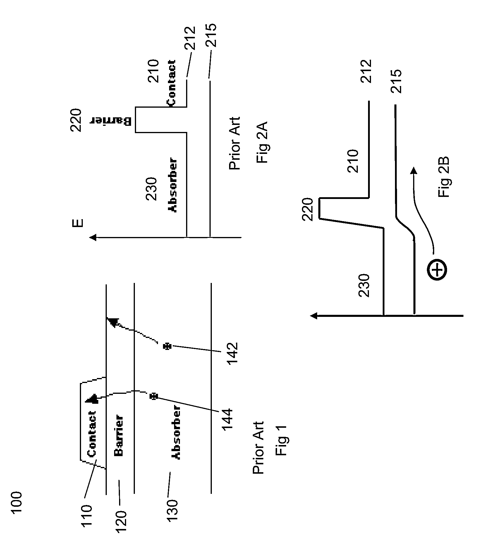
[0027]The following papers are incorporated by reference as though fully set forth herein: U.S. Pat. No. 7,687,871 Reduced Dark Current Photodetector by Shimon Maimon, issued 30 Mar. 2010.

[0028]In the following detailed description, only certain exemplary embodiments of the present invention are shown and described, by way of illustration. As those skilled in the art would recognize, the described exemplary embodiments may be modified in various ways, all without departing from the spirit or scope of the principles of the present invention. Accordingly, the drawings and description are to be regarded as illustrative in nature, and not restrictive.

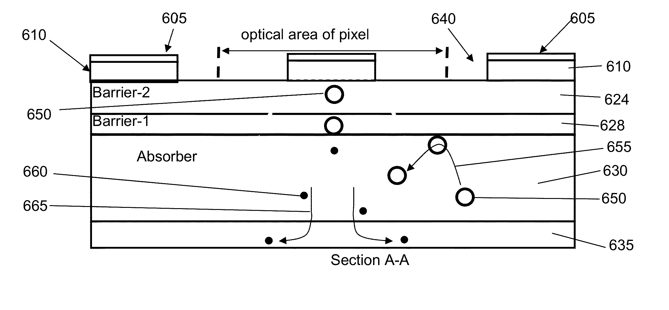
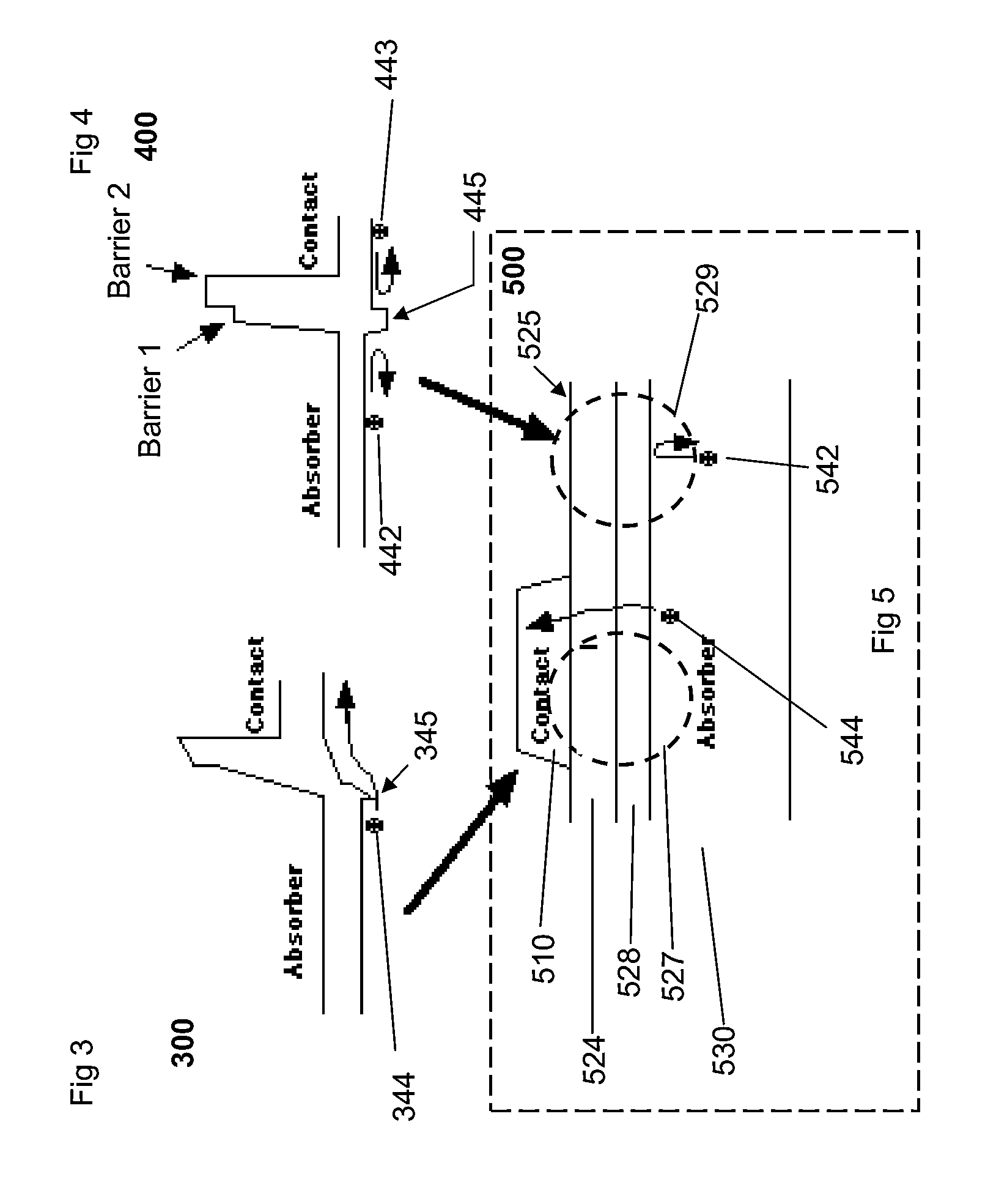
[0029]The problems described in the background section are at least partially solved by the principles of the present invention, including, by using a multiple layer barrier structure where each layer may be doped or undoped. The structure of an embodiment of the principles of the present invention uses a barrier structure comprising multip...


PUM


Abstract

Using a multiple layer, varied composition barrier layer in place of the typical single layer barrier layer of an infrared photodetector results in a device with increased sensitivity and reduced dark current. A first barrier is adjacent the semiconductor contact; a second barrier layer is between the first barrier layer and the absorber layer. The barrier layers may be doped N type or P type with Beryllium, Carbon, Silicon or Tellurium. The energy bandgap is designed to facilitate minority carrier current flow in the contact region and block minority current flow outside the contact region.

Description

[0001]This application claims priority to provisional application 61 / 351,368 filed Jun. 4, 2010 titled Compound Barrier Infrared Photodetector. Provisional application 61 / 351,368 is incorporated by reference herein. This application claims priority to provisional application 61 / 351,372 filed Jun. 4, 2010 titled Electrostatic Barrier Infrared Photodetector and incorporated by reference herein.STATEMENT REGARDING FEDERALLY SPONSORED RESEARCH OR DEVELOPMENT[0002]This invention was made with support from the United States Government under Contract No. S9 004726 awarded by the U.S. Government. The Government has certain rights in the invention.FIELD OF THE INVENTION[0003]The present technology relates to an apparatus and method for improving the sensitivity of a infrared photodetector while also reducing the dark current.BACKGROUND OF THE INVENTION[0004]Typical designs for an infrared photodetector for a focal plane array comprise a “barrier” layer of constant alloy composition, whose co...

Claims


Application Information

Patent Timeline
IPC IPC(8): H01L31/102
CPCH01L31/102Y02E10/544H01L31/101H01L27/146H01L31/109H01L31/0304H01L27/14649H01L31/0224H01L31/0328H01L31/0296H01L31/03046H01L31/035236H01L31/035272H01L31/111H01L31/1113H01L31/1116H01L27/14652H01L31/1035H01L31/11H01L31/1105H01L31/1844
Inventor DE LYON, TERENCE JRAJAVEL, RAJESH DSHARIFI, HASAN
Owner HRL LAB
Why Eureka
Try Eureka