Packaging system for protection of IC wafers during fabrication, transport and storage

a technology for packaging systems and integrated circuits, applied in the direction of packaging goods types, transportation and packaging, tray containers, etc., can solve problems such as surface components, bond pads, solder balls and interconnections which are susceptible to damag

Inactive Publication Date: 2014-10-21
BROOKS RAY G +1
View PDF16 Cites 9 Cited by
  • Summary
  • Abstract
  • Description
  • Claims
  • Application Information

AI Technical Summary

Benefits of technology

[0009]In accordance with another aspect, the wafers have edges subject to mechanical shock. The separators are sheets, the separators having peripheral rings located adjacent to the wafer edges so as to protect each associated packaged wafer edge from shock or physical damage.
[0012]In accordance with another aspect, at least one cushion is located in the wafer stack to absorb mechanical shock energy. The cushion comprises a compressible core and a flexible envelope around the core. The envelope has vents to allow gas to pass in and out of the top and bottom cushions at a controlled rate. The top and bottom cushions have sidewalls that compress when the top and bottom cushions are compressed. A flexible band is located around the side wall of at least one of the top and bottom cushions. The band is located outside of the cushion envelope and controls the flow of gas into and out of the respective cushion.

Problems solved by technology

The wafers have surface components such as bond pads, solder balls and interconnects which are susceptible to damage due to corrosion, mechanical shock and / or electrical static discharge.

Method used


Image

  • Packaging system for protection of IC wafers during fabrication, transport and storage
  • Packaging system for protection of IC wafers during fabrication, transport and storage
  • Packaging system for protection of IC wafers during fabrication, transport and storage

Examples


Embodiment Construction

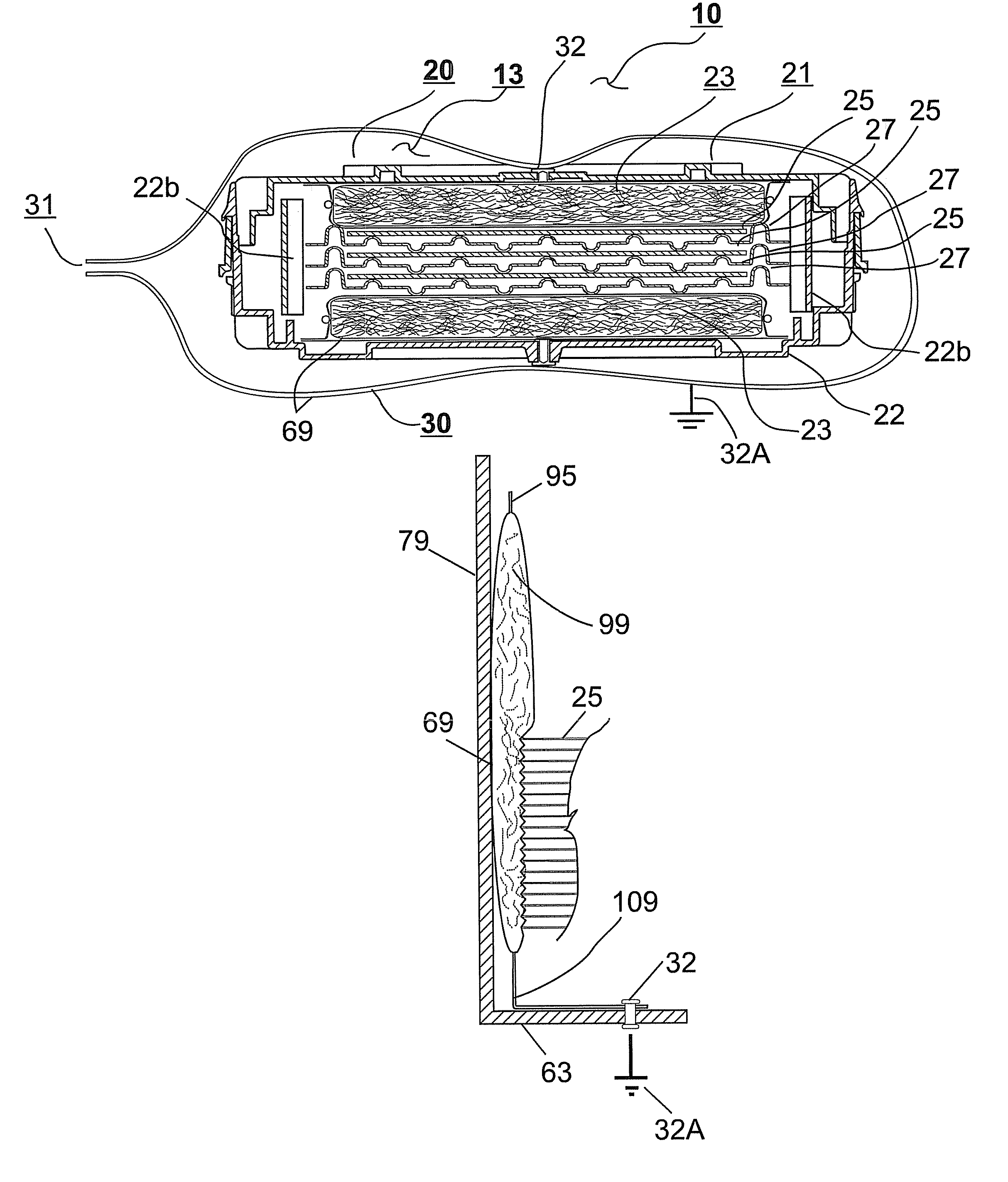
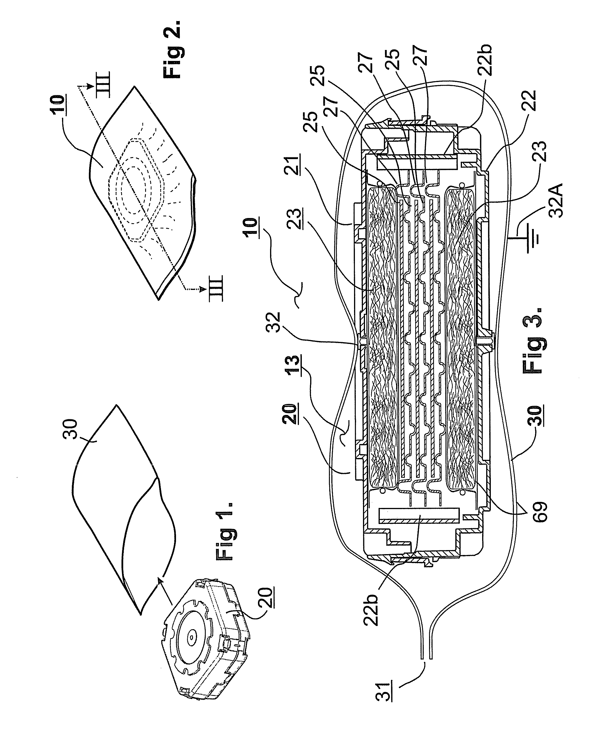
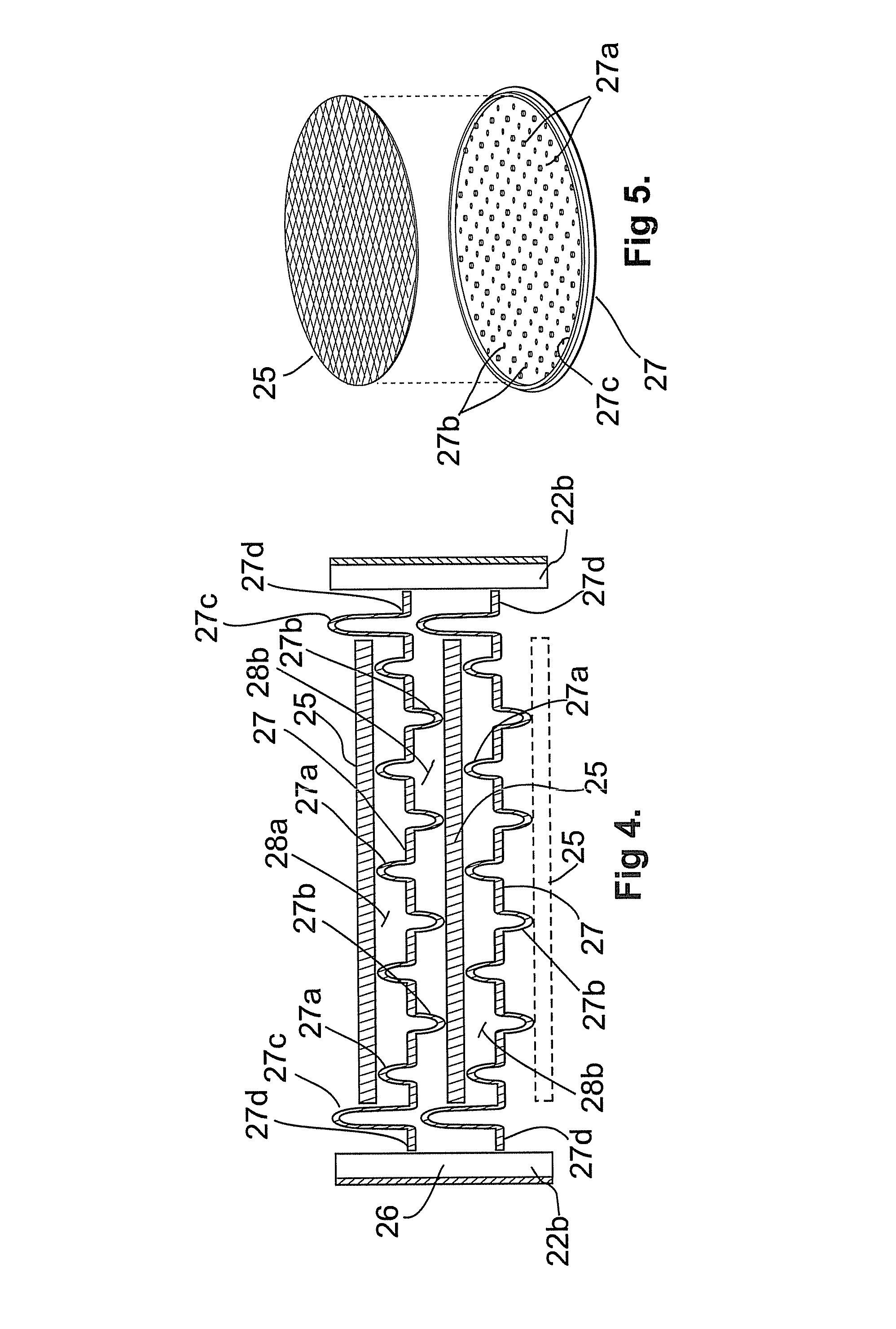
[0042]There is described a packaging system and method for protecting IC wafers during fabrication, transport and storage. The packaging system and method decrease IC wafer die losses by: 1) reducing contaminants that come into contact with the IC wafers, which contaminants cause corrosion damage; 2) absorbing mechanical shock energy, thereby reducing wafer breakage; and 3) providing electrical conductivity to dissipate electrostatic discharge.

[0043]Contaminants that damage IC wafers are airborne molecular contaminants (AMCs) and can be of the organic type and inorganic type. These AMCs move around and contaminate IC wafers using environmental moisture vapors. In an analogy, the moisture vapors are “taxi-cabs” that transport the AMCs throughout an environment. The system as described allows for the circulation of these moisture vapors throughout the packaging system and provides sacrificial surfaces intercept and capture these AMCs before the AMCs reach the IC wafers.

[0044]The prior...


PUM


Abstract

The packaging system includes an enclosure having an interior volume. A wafer stack, comprising plural wafers and separators in contact with the wafers, is located in the interior volume. The separators have raised bumps extending from each side. The bumps create spaces that allow air to flow therethrough. The separator film intercepts and captures airborne molecular contaminants belonging to organic and inorganic chemical families. In addition, the film is dissipative to static discharge. Furthermore, the bumps provided by the separators protect the fragile wafers from damage due to mechanical shock. The separators are also provided with a peripheral ring or embossment, which contacts the wafer edges and further protects the wafers from damage to mechanical shock. Air cushions can be provided in the wafer stack, which cushions are provided with bands to regulate the compression.

Description

[0001]This application claims the benefit of U.S. provisional application Ser. No. 61 / 434,194, filed Jan. 19, 2011.FIELD OF THE INVENTION[0002]The present invention relates to a packaging system for protecting integrated circuit (IC) wafers.BACKGROUND OF THE INVENTION[0003]Since the beginning of IC wafer fabrication, manufacturers have waged war against corrosive contaminants, relying on processing equipment within clean rooms having filters, monitors and / or mini-environments using containers identified as PODs, FOSBs (front opening shipping box) and / or FOUPs (front opening unified pod). These containers employ the concepts of Standard Mechanical Interface (SMIF). The clean rooms and containers have the purpose of significantly reducing IC die yield losses traceable to airborne molecular contaminants (AMCs). Examples of AMCs are HF (hafnium), HCL (hydrochloride) and VOC (volatile organic compounds). Although AMCs remain elusive, they are traceable to indoor and outdoor chemical acti...

Claims


Application Information

Patent Timeline
Patent Type & Authority Patents(United States)
IPC IPC(8): H01L21/673B65D85/48
CPCH01L21/67369H01L21/67396H01L21/67383
Inventor BROOKS, RAY G.BROOKS, TIMOTHY WAYNE
Owner BROOKS RAY G
Why Eureka
Try Eureka