Flip chip assembly apparatus employing a warpage-suppressor assembly

a technology of warpage suppressor and chip assembly, which is applied in the direction of soldering apparatus, manufacturing tools,auxillary welding devices, etc., can solve the problems of exacerbated mechanical stress caused by the mismatch between cte's, c4 balls or any other type of solder balls, and the connection employing an array of solder material portions is susceptible to mechanical stress, so as to facilitate the reflow of peripheral solder balls and prevent or minimize warpage of the contact substra

Active Publication Date: 2014-10-28
INT BUSINESS MASCH CORP
View PDF81 Cites 14 Cited by
  • Summary
  • Abstract
  • Description
  • Claims
  • Application Information

AI Technical Summary

Benefits of technology

[0006]A flip chip assembly apparatus includes at least one warpage-suppressor assembly. Each warpage-suppressor assembly can include a side heater, a deformable material pad, and an actuator assembly for moving the side heater and the deformable material pad. Each side heater provides additional heat to peripheral solder balls during bonding of two substrates, thereby facilitating the reflow of the peripheral solder balls. Each deformable material pad contacts, and presses down on, a surface of one of the two substrates under bonding. The deformable material pad(s) can prevent or minimize warpage of the contacted substrate.

Problems solved by technology

Connections employing an array of solder material portions, such as C4 balls or any other type of solder balls, are susceptible to mechanical stress created by a mismatch in the coefficients of thermal expansion (CTE's) between the semiconductor chip and the other semiconductor chip or the packaging substrate.
Such mechanical stress may cause cracks in the solder material portions, back-end-of-lines in chips, or the semiconductor chip(s), causing the semiconductor chip(s) to fail during flip chip assembly process and / or usage.
The problem of mechanical stress caused by the mismatch between CTE's are exacerbated when an organic substrate is employed for a packaging substrate because the mismatch of CTE's is greater between organic substrates and semiconductor substrates than between ceramic substrates and semiconductor substrates.
When an organic substrate is used as a packaging substrate for a fine pitch flip chip assembly, substrate warpage can occur in the conventional reflow process during which solder balls reflow.
This warpage can result in non-wetting of solder bumps and / or bridging between solder bumps, thereby decreasing the assembly yield.
Thermally-induced stress and strain in the flip-chip structure during a reflow process often results in a failure of back-end-of-line (BEOL) interconnect structures.
Even if the organic substrate is maintained below 100 degrees Celsius and the heat flow from the semiconductor chip into the organic substrate is constricted at the chip area during the reflow of the solder balls, the thermal expansion of the organic substrate is sufficient to cause warpage of the organic substrate.
Such warpage of the organic substrate tends to cause non-contacts between peripheral solder balls within the array of solder balls and bonding pads on the organic substrate, thereby causing electrical opens between the semiconductor chip and the organic substrate across the peripheral solder balls.

Method used


Image

  • Flip chip assembly apparatus employing a warpage-suppressor assembly
  • Flip chip assembly apparatus employing a warpage-suppressor assembly
  • Flip chip assembly apparatus employing a warpage-suppressor assembly

Examples


Embodiment Construction

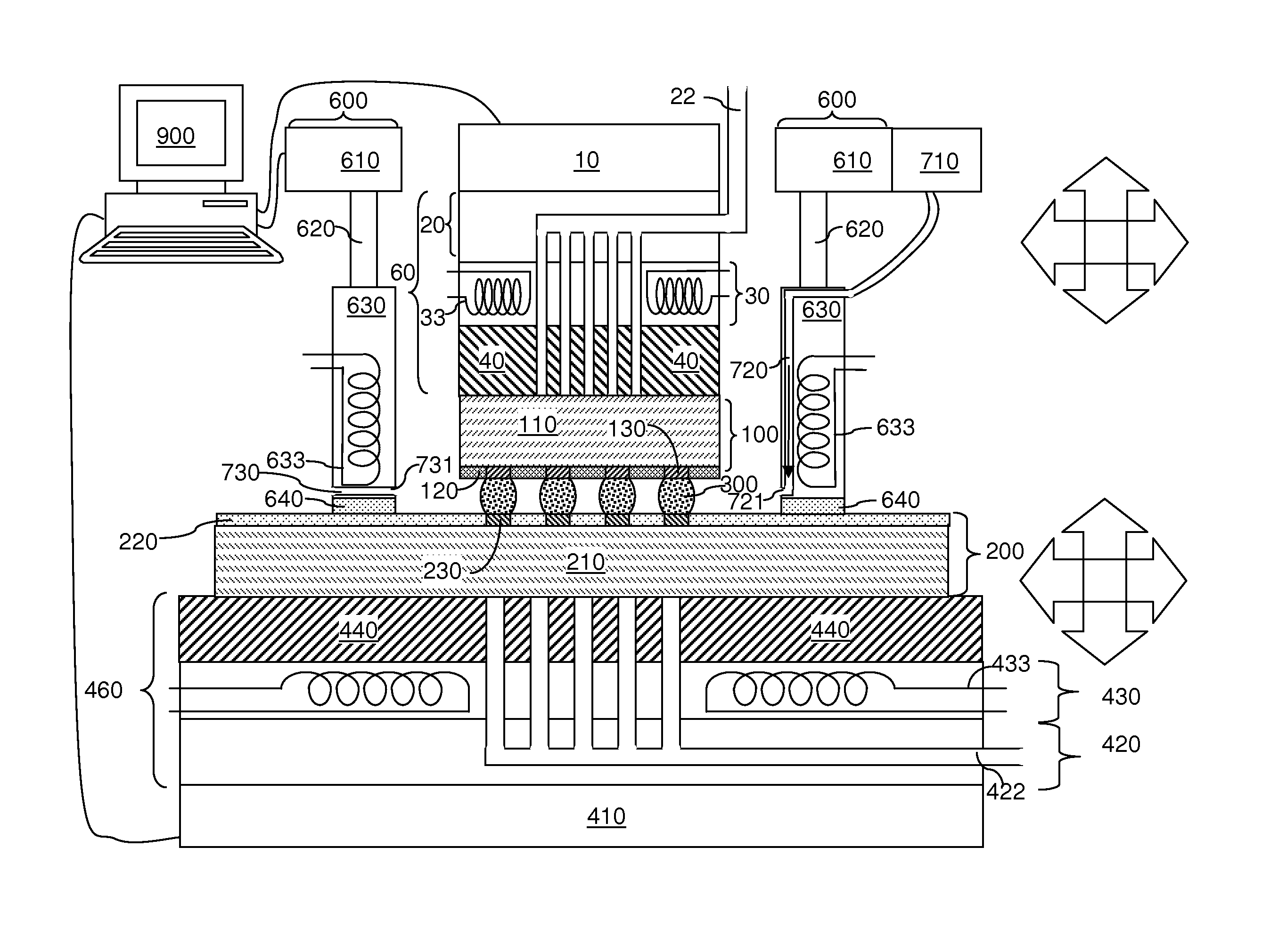
[0020]As stated above, the present disclosure relates to a flip chip assembly apparatus employing a warpage-suppressor assembly, and a method of operating the same, which are now described in detail with accompanying figures. It is noted that like and corresponding elements are referred to by like reference numerals. The drawings are not in scale.

[0021]Referring to FIGS. 1 and 2, an exemplary structure that can be employed for bonding a first substrate to a substrate according to an embodiment of the present disclosure is illustrated in a vertical cross-sectional view. The exemplary structure includes an exemplary bonding apparatus, which includes a bonder head 60, a base plate 460, and at least one warpage-suppressor assembly 600. The exemplary structure further includes a first substrate 100, an array of solder balls 300, and a second substrate 200. The exemplary apparatus can be employed for bonding the first substrate 100 to the second substrate 200.

[0022]The bonder head 60 is c...


PUM

PropertyMeasurementUnit
timeaaaaaaaaaa
temperatureaaaaaaaaaa

Abstract

A flip chip assembly apparatus includes at least one warpage-suppressor assembly. Each warpage-suppressor assembly can include a side heater, a deformable material pad, and an actuator assembly for moving the side heater and the deformable material pad. Each side heater provides additional heat to peripheral solder balls during bonding of two substrates, thereby facilitating the reflow of the peripheral solder balls. Each deformable material pad contacts, and presses down on, a surface of one of the two substrates under bonding. The deformable material pad(s) can prevent or minimize warpage of the contacted substrate.

Description

BACKGROUND[0001]The present disclosure relates to a method for bonding substrates, and particularly, to a flip chip assembly apparatus employing a warpage-suppressor assembly, and a method of operating the same.[0002]Connections employing an array of solder material portions, such as C4 balls or any other type of solder balls, are susceptible to mechanical stress created by a mismatch in the coefficients of thermal expansion (CTE's) between the semiconductor chip and the other semiconductor chip or the packaging substrate. Such mechanical stress may cause cracks in the solder material portions, back-end-of-lines in chips, or the semiconductor chip(s), causing the semiconductor chip(s) to fail during flip chip assembly process and / or usage.[0003]The problem of mechanical stress caused by the mismatch between CTE's are exacerbated when an organic substrate is employed for a packaging substrate because the mismatch of CTE's is greater between organic substrates and semiconductor substr...

Claims


Application Information

Patent Timeline
Patent Type & Authority Patents(United States)
IPC IPC(8): B23K37/04
CPCH01L24/81B23K37/04B23K31/02H01L2924/10253B23K1/0016B23K3/047B23K35/0244B23K2201/40H01L2924/1305H01L2924/15787B23K35/0222B23K2101/40H01L2924/00
Inventor BROFMAN, PETER J.NAH, JAE-WOONGSAKUMA, KATSUYUKI
Owner INT BUSINESS MASCH CORP
Why Eureka
Try Eureka