
Line-edge roughness improvement for small pitches

a technology of micro-pitch and micro-pitch, applied in the field of micro-pitch improvement of micro-pitch, can solve the problems of rough and potentially uneven hard areas of the photoresist, the phenomenon of line-edge roughness is now a serious problem, and the photoresist in ultra-violet lithography exacerbates the problem of line-edge roughness, so as to reduce film stress differences and mitigate the extent of line-edge roughness

Active Publication Date: 2014-11-04
SPANSION LLC
View PDF6 Cites 2 Cited by
  • Summary
  • Abstract
  • Description
  • Claims
  • Application Information

AI Technical Summary

Benefits of technology

This patent discusses a solution for dealing with issues in creating structures with small NAND pitches. It focuses on reducing line-edge roughness and line wiggling. The text identifies several techniques to mitigate these issues, such as reducing film stress differences and reducing the attack or distortion of the photoresist during plasma etching.

Problems solved by technology

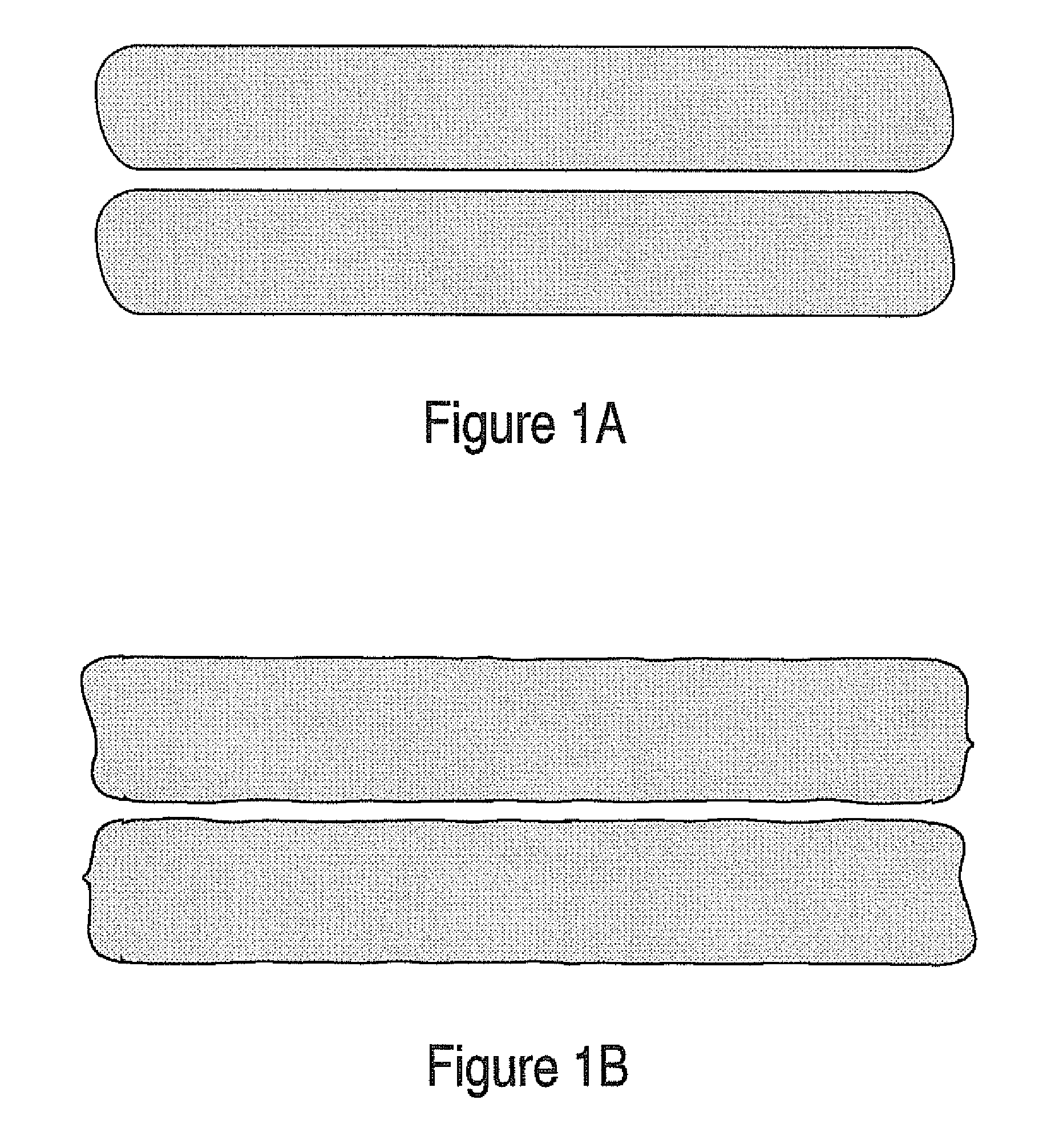
With the use of ArF photoresist in ultra violet lithography and pitch sizes dropping below 100 nm, the phenomenon of line-edge roughness is now a serious problem.
The use of ArF photoresist in ultra violet lithography exacerbates the problem of line-edge roughness.
Ultra violet photoresist's sensitivity to plasma causes distortions in the resist line as the etching process continues, and therefore, forming the line edges of trenches and other structures underneath the photoresist with distortions transferred from the photoresist.
When atomic effects begin to play a part in the quality of line edges, the clusters of polymers that may form in the photoresist now lead to deformities that may be seen in tight line edges.
The softer areas of the photoresist are more easily etched away, leaving behind rough and potentially uneven harder areas of the photoresist.
The plasma etching process further distorts the photoresist by heating it and changing its chemical components, causing a stress change in the resist.
The lines patterned in the photoresist react to that stress change resulting in a buckling of the photoresist, with all of these affects becoming more visible and problematic as pitch sizes shrink with each technological generation.
A thin resist is more easily patterned, but is also more vulnerable to the damaging effects of etching.
Further, the etching process itself reduces the photoresist mask during etching.
The end result is devices that don't work.
The increased line-edge roughness results in whole chips that don't work because of roughness causing crude defects such as shorts and breaks in the copper lines formed in the trenches etched through the patterned resist lines.
However, with pitches smaller than 100 nm, even low levels of line-edge roughness are producing unacceptable results and new solutions are needed.

Method used


Image

  • Line-edge roughness improvement for small pitches
  • Line-edge roughness improvement for small pitches
  • Line-edge roughness improvement for small pitches

Examples


Embodiment Construction

[0026]Reference will now be made in detail to the preferred embodiments of the present invention, examples of which are illustrated in the accompanying drawings. While the invention will be described in conjunction with the preferred embodiments, it will be understood that they are not intended to limit the invention to these embodiments. On the contrary, the invention is intended to cover alternatives, modifications and equivalents, which may be included within the spirit and scope of the invention as defined by the appended claims. Furthermore, in the following detailed description of embodiments of the present invention, numerous specific details are set forth in order to provide a thorough understanding of the present invention. However, it will be recognized by one of ordinary skill in the art that the present invention may be practiced without these specific details. In other instances, well-known methods, procedures, components, and circuits have not been described in detail ...


PUM


Abstract

A method for mitigating line-edge roughness on a semiconductor device. The method includes line-edge roughness mitigation techniques in accordance with embodiments of the present invention. The techniques include: reducing the SiON film thickness below a conventional thickness; increasing the photoresist thickness above a conventional thickness; etching the SiON film with an etch bias power less than a conventional wattage amount with an overetch percentage less than a conventional overetch percentage; removing the SiON film layer immediately after completion of the amorphous carbon film layer etching; and lowering the lower electrode temperature below a conventional temperature.

Description

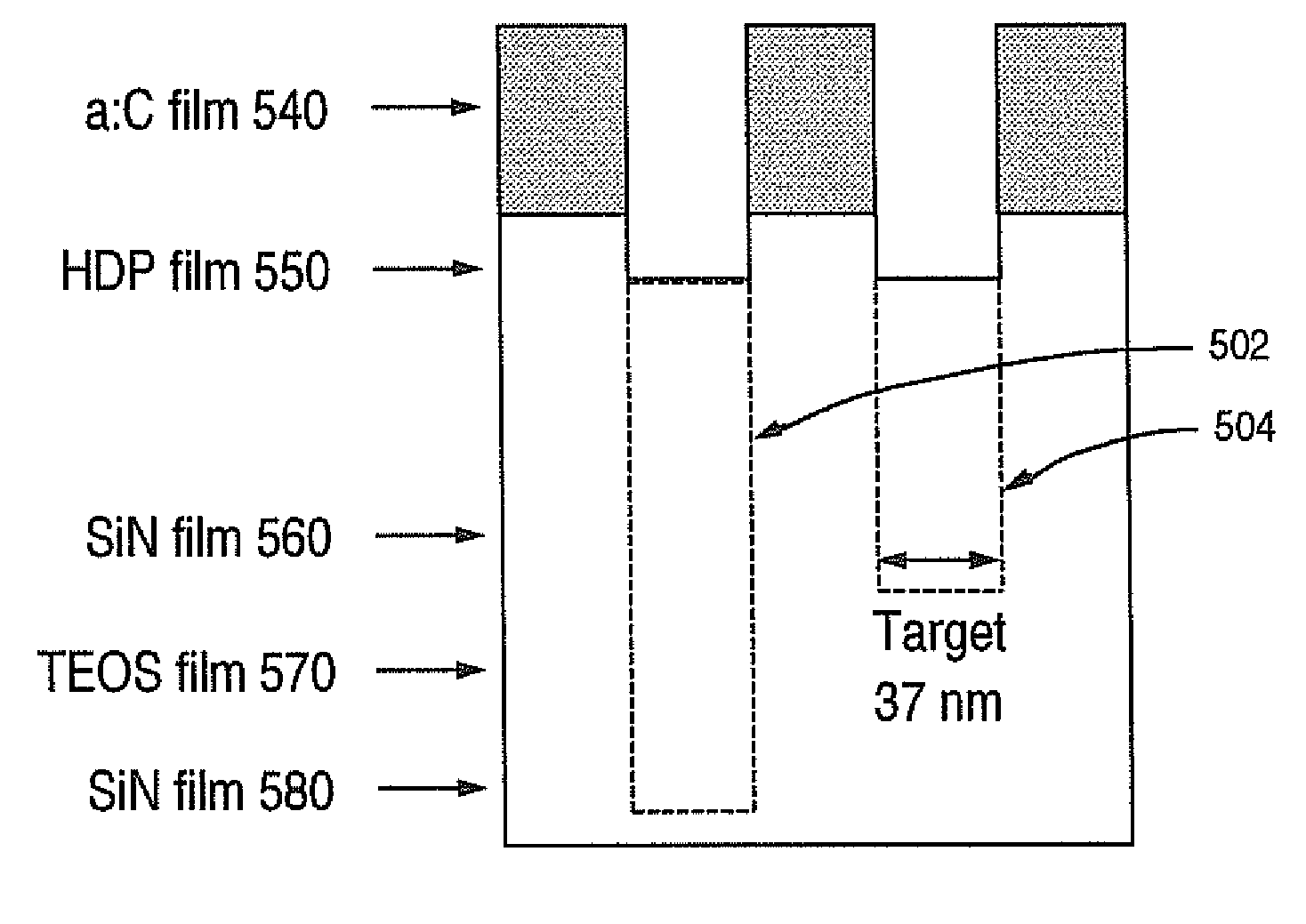
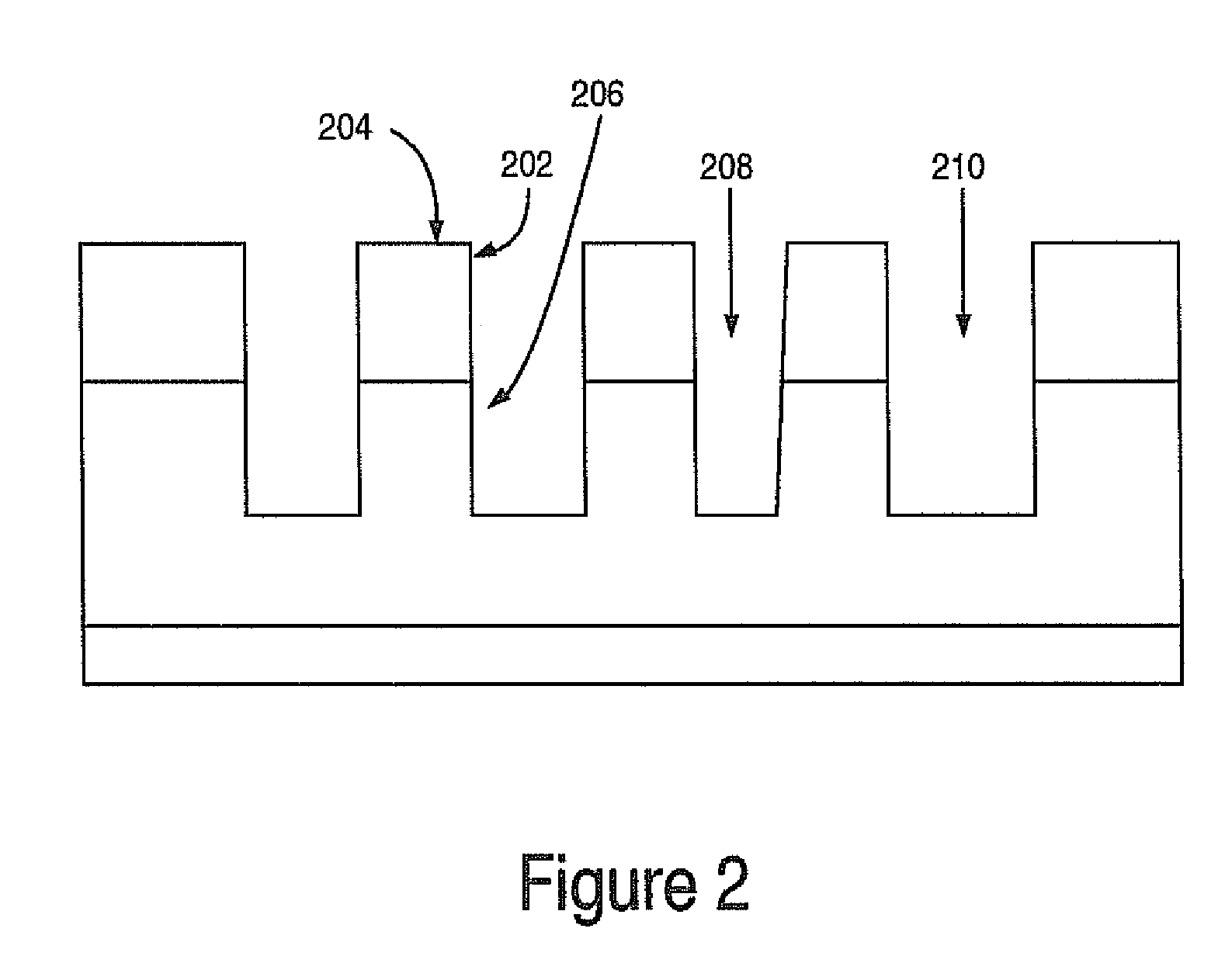
TECHNICAL FIELD[0001]The present invention relates generally to semiconductor substrate processing. More particularly to reducing line-edge roughness seen along line edges of trenches and other structures formed in semiconductor devices.BACKGROUND[0002]Efforts of the semiconductor fabricating industry to produce continuing improvements in miniaturization and packing densities has seen improvements and new challenges to the semiconductor fabricating process. One example semiconductor process experiencing tremendous improvements in miniaturization and packing densities is ultra-violet lithography. Making use of the pattern transfer ability of photoresist materials formed into patterns through lithography exposure and developing, semiconductor pitch sizes have fallen steadily. Today lithography techniques patterning with 193 nanometer (nm) Argon Fluoride (ArF) photoresists are enabling process technologies to reach pitch structures as small as 43 nm and 32 nm NAND. The “pitch” of a sem...

Claims


Application Information

Patent Timeline
Patent Type & Authority Patents(United States)
IPC IPC(8): H01L21/302H01L21/768H01L21/311
CPCH01L21/31144H01L21/76802H01L21/31116H01L21/3065H01L21/31138
Inventor GABRIEL, CALVIN, T
Owner SPANSION LLC
Learn More