Plasma processing apparatus and electrode for same

a technology of processing apparatus and electrode, which is applied in the direction of coating, chemical vapor deposition coating, electric discharge tubes, etc., can solve the problems of stress concentration, lack of machining accuracy, and deterioration of dimensional accuracy at the tapered portion

Active Publication Date: 2014-11-18
TOKYO ELECTRON LTD
View PDF19 Cites 0 Cited by
  • Summary
  • Abstract
  • Description
  • Claims
  • Application Information

AI Technical Summary

Benefits of technology

[0012]In view of the above, the present invention provides a plasma processing apparatus that may control an electric field strength distribution at the plasma-side surface of a parallel plate type electrode and an electrode for the plasma processing apparatus.
[0014]With such configuration, when a high frequency current flows along the metal surface of the base, the high frequency energy is distributed due to capacitance caused by volume of the first dielectric material provided at the central portion of the electrode. As a result, the electric field strength of an electromagnetic field generated by propagation of high frequency current through the central portion of the electrode becomes lower in a case where there is a dielectric material than in a case where there is no dielectric material. In addition, the first resistor with a predetermined pattern is provided between the first dielectric material and plasma. This allows the high frequency current to flow along the skin of the first resistor as well as along the metal surface of the base. The high frequency energy is partially converted into Joule heat due to the resistance of the first resistor while the current flows through the first resistor and the converted Joule heat is consumed, thus creating a potential distribution due to the current and resistance. This makes it possible to gradually lower the high frequency electric field strength at the position where the first resistor is arranged.
[0015]As the impedance at the electrode side increases, the electric field energy consumed for plasma decreases. In the electrode according to the present invention, thus, the position and capacitance C of the first dielectric material and the position and resistance R of the first resistor are set so that the impedance at the central portion of the electrode is gradually increased compared to the impedance at the end portion of the electrode. By doing so, it may be possible to make the electric field strength uniform at the bottom portion of the electrode, thereby generating plasma with uniform plasma density Ne.
[0016]Further, since there is no need of making the first dielectric material tapered, machining costs may be saved. Due to a discrepancy in dimensional tolerance and difference in thickness of dielectric material, stress concentration conventionally occurred and this caused the adhesive or sprayed material to be peeled off. The peeling was a cause of contamination. In the construction according to the present invention, however, the first dielectric material does not necessarily have a tapered shape, thus capable of reducing peeling of the adhesive or sprayed material and suppressing contamination.
[0030]As described above, the present invention may control the electric field strength distribution on the plasma side surface of the parallel plate type electrode.

Problems solved by technology

If the dielectric material 915 has a tapered shape, the dimensional accuracy is deteriorated at the tapered portion due to a lack of machining accuracy.
This results in stress concentration due to a difference in heat expansion.
Since the difference in thermal expansion coefficient makes it difficult to manage the gap due to a difference in heat expansion, the peeled adhesive escapes from the gap, which causes a contamination in the chamber.

Method used


Image

  • Plasma processing apparatus and electrode for same
  • Plasma processing apparatus and electrode for same
  • Plasma processing apparatus and electrode for same

Examples


Embodiment Construction

[0059]Hereinafter, embodiments of the present invention will be described in detail with reference to accompanying drawings which form a part hereof. Through the specification, like reference numerals refer to like elements and the repetitive descriptions will be omitted.

[0060](1) The Entire Construction of the Plasma Processing Apparatus

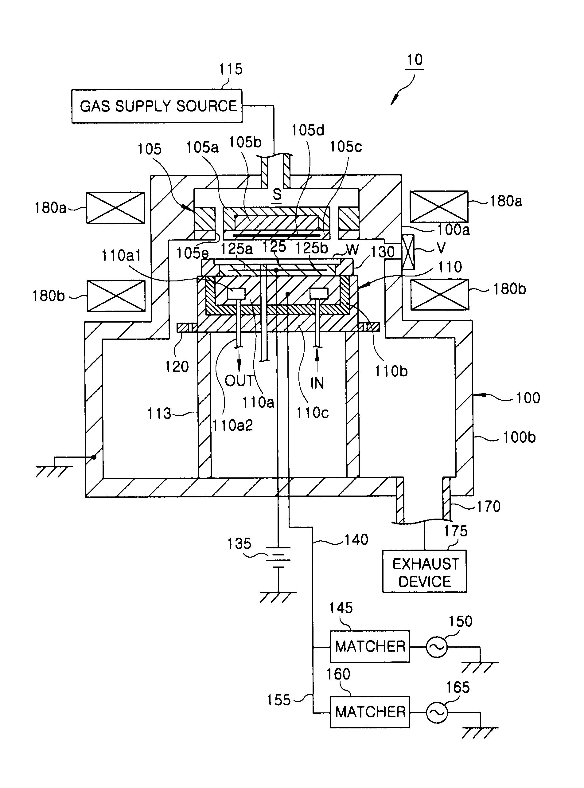
[0061]First of all, the entire construction of a plasma processing apparatus having an electrode according to an embodiment of the present invention will be described with reference to FIG. 1. FIG. 1 depicts a RIE (Reactive Ion Etching) plasma etching apparatus (parallel plate type plasma processing apparatus) having an electrode according to an embodiment of the present invention. The RIE (Reactive Ion Etching) plasma etching apparatus 10 corresponds to a plasma processing apparatus that generates plasma by a high frequency energy and plasma processes a wafer W.

[0062]The RIE plasma etching apparatus 10 includes a processing chamber 100 that plasma ...


PUM

PropertyMeasurementUnit
frequencyaaaaaaaaaa
thicknessaaaaaaaaaa
diameteraaaaaaaaaa

Abstract

A plasma processing apparatus includes a processing chamber that plasma processes a target object therein, first and second electrodes that are provided in the processing chamber to face each other and have a processing space therebetween, and a high frequency power source that is connected to at least one of the first and second electrodes to supply high frequency power to the processing chamber. At least one of the first and second electrodes includes a base formed of a metal, a dielectric material provided at a central portion of a plasma side of the base, and a first resistor provided between the dielectric material and plasma, and formed of a metal with a predetermined pattern.

Description

CROSS-REFERENCE TO RELATED APPLICATIONS[0001]This application claims priority to Japanese Patent Application No. 2009-053423 filed on Mar. 6, 2009, the entire contents of which are incorporated herein by reference.FIELD OF THE INVENTION[0002]The present invention is related to a structure of an electrode used for a plasma processing apparatus and a plasma processing apparatus using same; and, more specifically, to a structure of an electrode for a plasma processing apparatus that may control the distribution of an electric field strength consumed by high frequency power for a generation of plasma between parallel plate type electrodes.BACKGROUND OF THE INVENTION[0003]As apparatuses become commercially available for performing microprocessing, e.g., etching or film forming, on a target object by plasma action, capacitively coupled (parallel plate type) plasma processing apparatuses, inductively coupled plasma processing apparatuses, and microwave plasma processing apparatuses are com...

Claims


Application Information

Patent Timeline
Patent Type & Authority Patents(United States)
IPC IPC(8): H01J37/32C23F1/00H01L21/306C23C16/00
CPCH01J2237/03H01J37/32577H01J37/3255H01L21/3065H05H1/34C23C14/34H01L21/02631
Inventor HIMORI, SHINJI
Owner TOKYO ELECTRON LTD
Why Eureka
Try Eureka