
Semiconductor device

a semiconductor and device technology, applied in the direction of transistors, solid-state devices, instruments, etc., can solve the problems of degradation of the field-effect mobility of the transistor, etc., and achieve the effect of high field-effect mobility, high reliability of the semiconductor device, and the prevention of change in the electrical characteristics of the transistor including the oxide semiconductor

Active Publication Date: 2014-12-02
SEMICON ENERGY LAB CO LTD
View PDF171 Cites 54 Cited by
  • Summary
  • Abstract
  • Description
  • Claims
  • Application Information

AI Technical Summary

Benefits of technology

The present invention aims to provide a semiconductor device with high field-effect mobility that includes an oxide semiconductor. Additionally, it aims to prevent changes in the electrical characteristics of a transistor with an oxide semiconductor to create a more reliable semiconductor device.

Problems solved by technology

For example, interface scattering of carriers at the interface between the oxide semiconductor layer and the insulating layer in contact with the oxide semiconductor layer causes degradation of the field-effect mobility of the transistor.
The impurity mixed into the channel causes degradation of the electrical characteristics of the transistor.

Method used


Image

  • Semiconductor device
  • Semiconductor device
  • Semiconductor device

Examples


embodiment 1

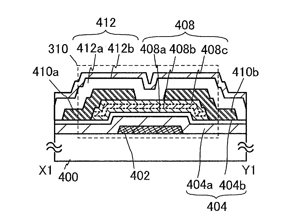
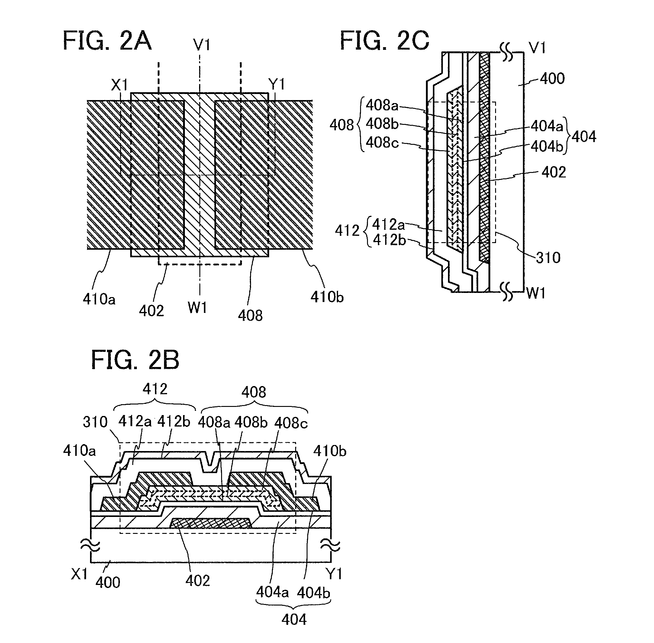
[0058]In this embodiment, one embodiment of a semiconductor device and one embodiment of a method for manufacturing the semiconductor device will be described with reference to FIGS. 2A to 2C and FIGS. 3A to 3E. In this embodiment, a bottom-gate transistor including an oxide semiconductor layer is described as an example of the semiconductor device.

[0059]FIG. 2A illustrates a structural example of a transistor 310. The transistor 310 in FIG. 2A includes a gate electrode layer 402 provided over a substrate 400 having an insulating surface, a gate insulating layer 404 over the gate electrode layer 402, an oxide semiconductor stack 408 which is in contact with the gate insulating layer 404 and overlaps with the gate electrode layer 402, and a source electrode layer 410a and a drain electrode layer 410b which are electrically connected to the oxide semiconductor stack 408. Further, an insulating layer 412 which covers the source electrode layer 410a and the drain electrode layer 410b an...

embodiment 2

[0142]In this embodiment, one embodiment of a semiconductor device which is different from that in Embodiment 1 will be described with reference to FIGS. 12A and 12B.

[0143]FIG. 12A illustrates a structural example of a transistor 320. In a manner similar to the transistor 310 in FIGS. 2A to 2C, the transistor 320 in FIG. 12A includes the gate electrode layer 402 provided over the substrate 400 having an insulating surface, the gate insulating layer 404 over the gate electrode layer 402, an oxide semiconductor stack which is in contact with the gate insulating layer 404 and overlaps with the gate electrode layer 402, and the source electrode layer 410a and the drain electrode layer 410b which are electrically connected to the oxide semiconductor stack. Further, the insulating layer 412 which covers the source electrode layer 410a and the drain electrode layer 410b and is in contact with the oxide semiconductor stack may be included as a component of the transistor 320.

[0144]An oxide ...

embodiment 3

[0163]In this embodiment, a CAAC-OS film which can be used as an oxide semiconductor layer will be described. Specifically, a phenomenon which occurs during formation of a CAAC-OS film is described in detail with reference to FIGS. 13A to 13C, FIGS. 14A and 14B, and FIGS. 15A to 15C.

[0164]As described above, during deposition, fine sputtered particles fly from a target, and a film is formed such that the sputtered particles adhere onto the deposition-target substrate. When the temperature of the substrate is higher than or equal to 200° C., the sputtered particles are rearranged because the substrate is heated. Thus, a dense film is formed.

[0165]When ions collide with the surface of the sputtering target, a crystal region included in the sputtering target is cleaved along an a-b plane, and sputtered particles whose top and bottom surfaces are each aligned with a layer parallel to the a-b plane (flat-plate-like sputtered particle or pellet-like sputtered particle) are separated from ...


PUM


Abstract

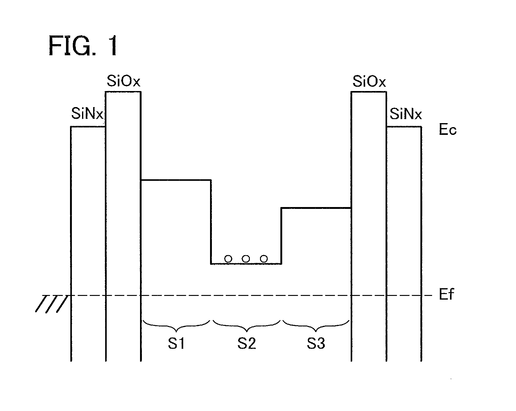
High field-effect mobility is provided for a transistor including an oxide semiconductor. Further, a highly reliable semiconductor device including the transistor is provided. In a bottom-gate transistor including an oxide semiconductor layer, an oxide semiconductor layer functioning as a current path (channel) of the transistor is sandwiched between oxide semiconductor layers having lower carrier densities than the oxide semiconductor layer. In such a structure, the channel is formed away from the interface of the oxide semiconductor stacked layer with an insulating layer in contact with the oxide semiconductor stacked layer, i.e., a buried channel is formed.

Description

BACKGROUND OF THE INVENTION[0001]1. Field of the Invention[0002]The invention disclosed in this specification and the like relates to a semiconductor device and a method for manufacturing the semiconductor device.[0003]In this specification and the like, a semiconductor device refers to all types of devices which can function by utilizing semiconductor characteristics; an electro-optical device, an image display device, a semiconductor circuit, and an electronic device are all semiconductor devices.[0004]2. Description of the Related Art[0005]A technique by which transistors are formed using semiconductor thin films formed over a substrate having an insulating surface has been attracting attention. Such a transistor is applied to a wide range of electronic devices such as an integrated circuit (IC) and an image display device (also simply referred to as a display device). A silicon-based semiconductor material is widely known as a material for a semiconductor thin film applicable to...

Claims


Application Information

Patent Timeline
Patent Type & Authority Patents(United States)
IPC IPC(8): H01L29/786H01L29/12H01L29/36
CPCH01L29/78693H01L29/78696H01L29/7869H01L29/267H01L29/512H01L29/518H01L27/14616H01L27/14612H10K59/65H01L27/1225H01L29/06H10K59/40G06F3/0412G06F3/04886H01L29/4908H01L31/03762H01L31/103
Inventor YAMAZAKI, SHUNPEI
Owner SEMICON ENERGY LAB CO LTD
Learn More