
Methods involving color-aware retargeting of individual decomposed patterns when designing masks to be used in multiple patterning processes

a pattern and pattern technology, applied in the field of semiconductor devices, can solve the problems of inability to accept variations in topography, design and manufacture of reticles used in such photolithography processes, and the accuracy of pattern transfer in photolithography processes has become even more important and more difficul

Inactive Publication Date: 2014-12-30
GLOBALFOUNDRIES INC
View PDF7 Cites 104 Cited by
  • Summary
  • Abstract
  • Description
  • Claims
  • Application Information

AI Technical Summary

Benefits of technology

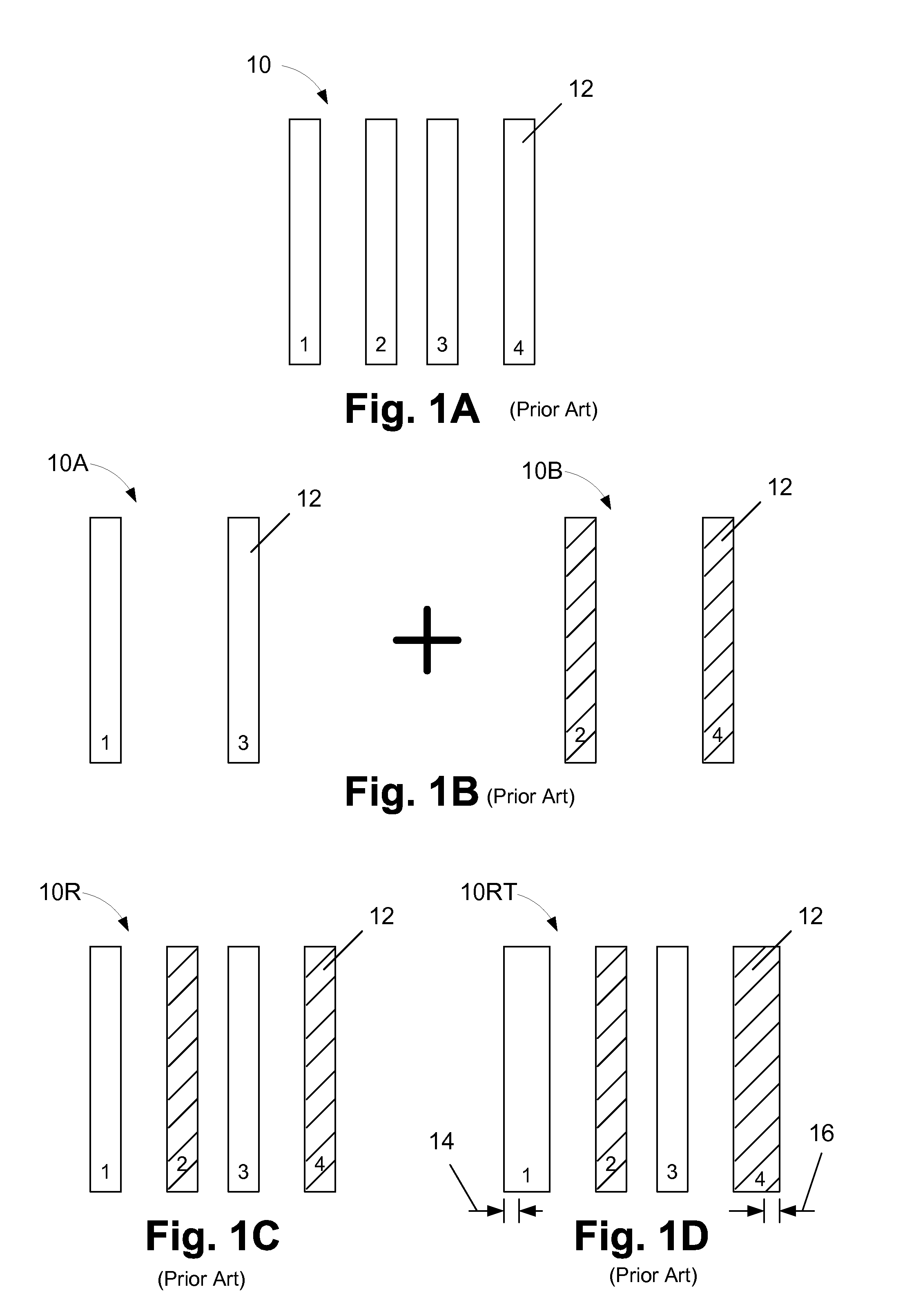
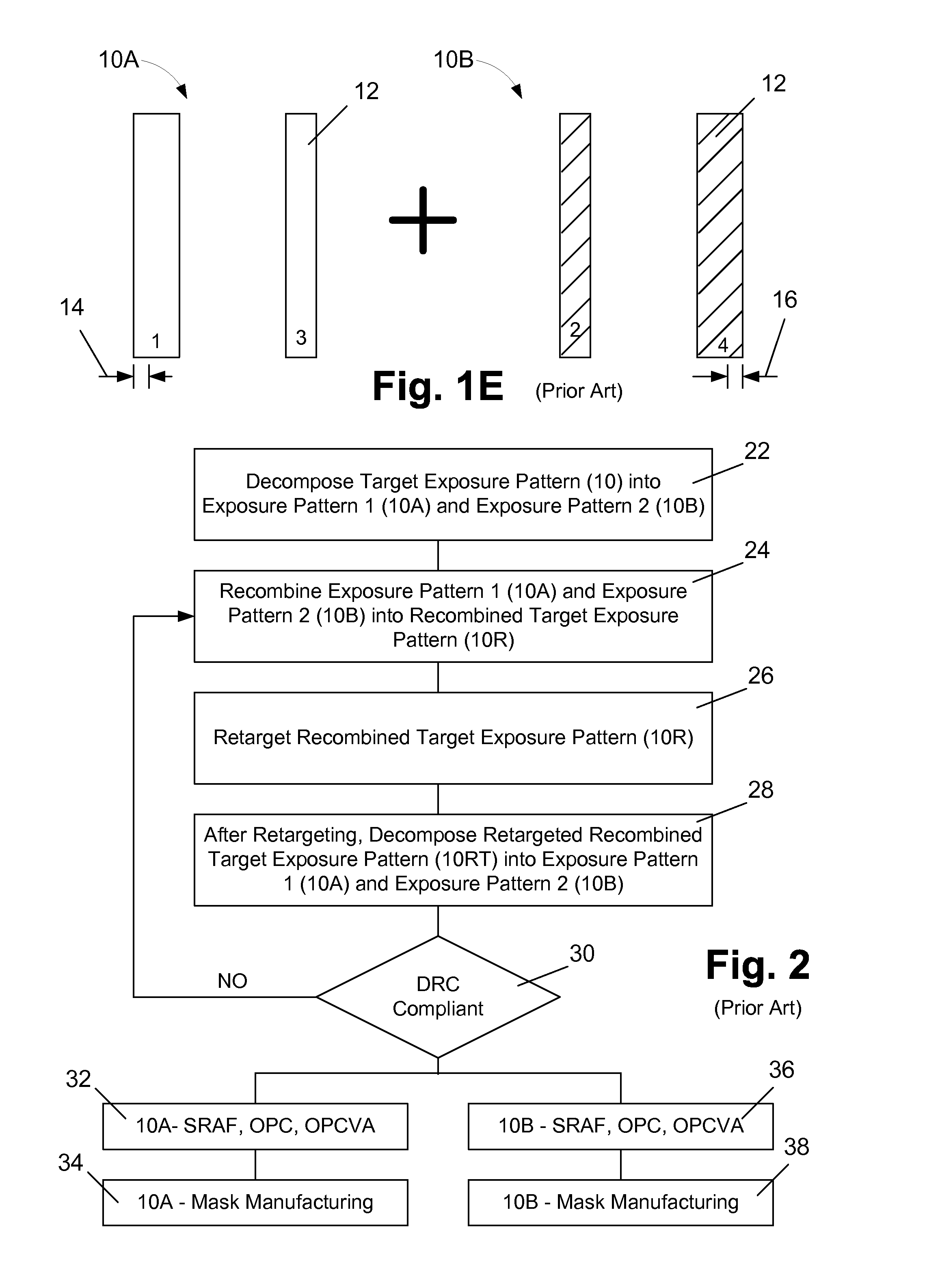
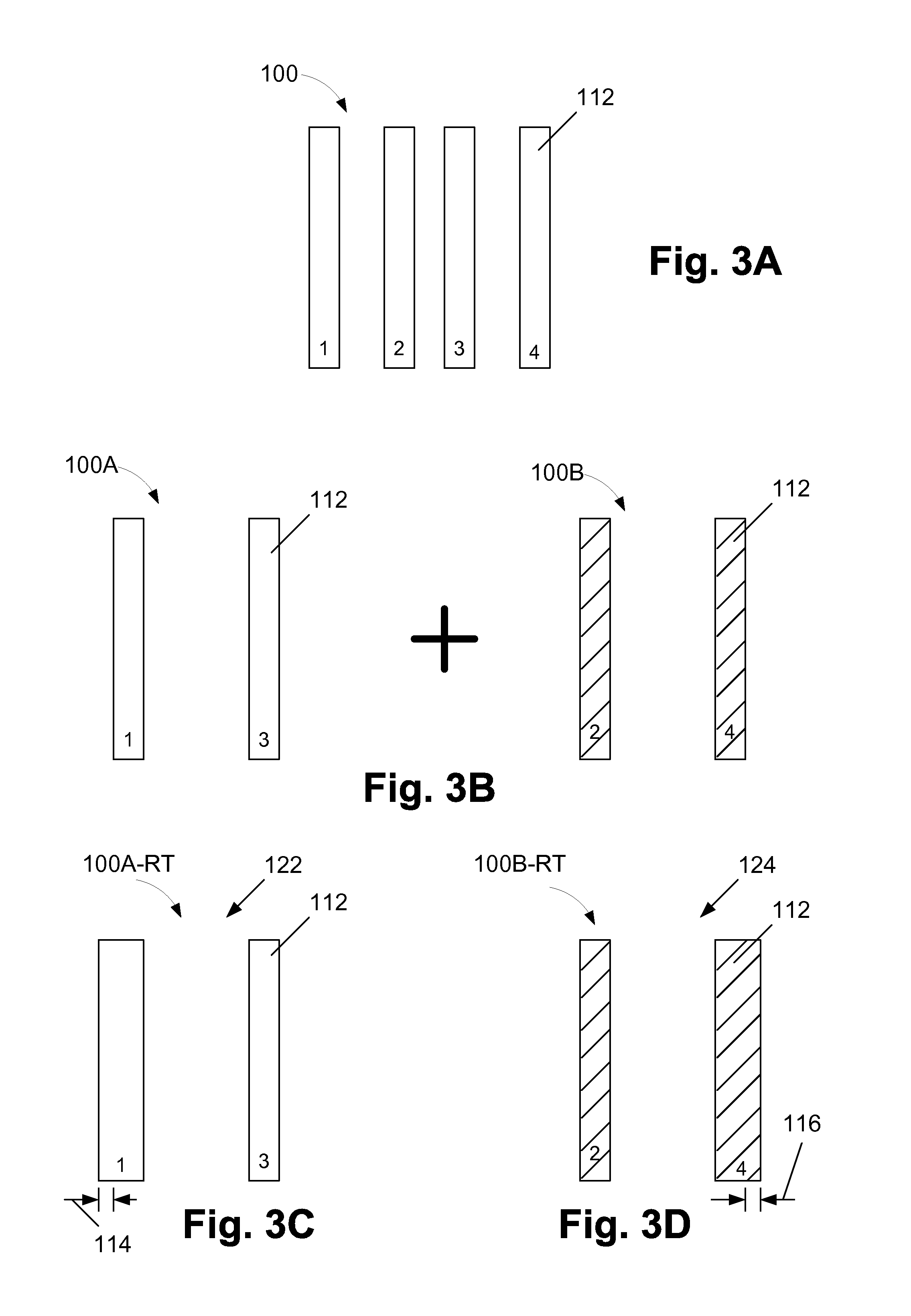
The present disclosure describes methods for designing masks or reticles used in multiple patterning processes to manufacture integrated circuit products. These methods involve decomposing an initial target exposure pattern into sub-target patterns, performing retargeting processes on each decomposed sub-target pattern to define a retargeted sub-target pattern, and checking if the retargeted patterns are in compliance with design rules. The technical effects of this invention include improved accuracy and precision in designing masks or reticles, and better manufacturing of integrated circuit products.

Problems solved by technology

The design and manufacture of reticles used in such photolithography processes is a very complex and expensive undertaking as such masks must be very precise and must enable the repeated and accurate formation of a desired pattern in the underlying layer of material (for an etching process).
There are several factors that cause such printing differences, such as interference between light beams transmitted through adjacent patterns, resist processes, the reflection of light from adjacent or underlying materials or structures, unacceptable variations in topography, etc.
In recent years, the accuracy of pattern transfer in photolithography processes has become even more important and more difficult due to, among other things, the ongoing shrinkage of various features on integrated circuit devices.
However, in recent years, device dimensions and pitches have been reduced to the point where existing photolithography tools, e.g., 193 nm wavelength photolithography tools, cannot perform a single exposure process to form a single patterned mask layer that will enable the formation of all of the desired features of the overall target pattern.
Despite all of these techniques, the lithography process that is exerted to a point at or near its limits will still not allow all patterns to be faithfully reproduced on the wafer in the presence of normal manufacturing process variations.
These rules are set by processing and design limitations.

Method used


Image

  • Methods involving color-aware retargeting of individual decomposed patterns when designing masks to be used in multiple patterning processes
  • Methods involving color-aware retargeting of individual decomposed patterns when designing masks to be used in multiple patterning processes
  • Methods involving color-aware retargeting of individual decomposed patterns when designing masks to be used in multiple patterning processes

Examples


Embodiment Construction

[0024]Various illustrative embodiments of the invention are described below. In the interest of clarity, not all features of an actual implementation are described in this specification. It will of course be appreciated that in the development of any such actual embodiment, numerous implementation-specific decisions must be made to achieve the developers' specific goals, such as compliance with system-related and business-related constraints, which will vary from one implementation to another. Moreover, it will be appreciated that such a development effort might be complex and time-consuming, but would nevertheless be a routine undertaking for those of ordinary skill in the art having the benefit of this disclosure.

[0025]The present subject matter will now be described with reference to the attached figures. Various structures, systems and devices are schematically depicted in the drawings for purposes of explanation only and so as to not obscure the present disclosure with details ...


PUM

PropertyMeasurementUnit
sizeaaaaaaaaaa
optical proximityaaaaaaaaaa
lengthsaaaaaaaaaa

Abstract

One illustrative method disclosed herein includes the steps of decomposing an initial overall target exposure pattern into at least a first decomposed sub-target pattern and a second decomposed sub-target pattern, performing first and second retargeting processes on the first and second decomposed sub-target patterns while using the other sub-target pattern as a reference layer, respectively, to thereby define retargeted first and second decomposed sub-target patterns, respectively, and, after performing the first and second retargeting processes, performing at least one process operation to determine if each of the retargeted first decomposed sub-target pattern and the retargeted second decomposed sub-target pattern is in compliance with at least one design rule.

Description

BACKGROUND OF THE INVENTION[0001]1. Field of the Invention[0002]Generally, the present disclosure relates to the manufacture of semiconductor devices, and, more specifically, to various methods that involve color-aware retargeting of individual decomposed patterns when designing masks or reticles to be used in multiple patterning processes, such as double patterning processes, and the use of such masks or reticles in various photolithography systems to manufacture integrated circuit products.[0003]2. Description of the Related Art[0004]Photolithography is one of the basic processes used in manufacturing integrated circuit products. At a very high level, photolithography involves (1) forming a layer of light or radiation-sensitive material, such as photoresist, above a layer of material or a substrate, (2) selectively exposing the radiation-sensitive material to a light generated by a light source (such as a DUV or EUV source) to transfer a pattern defined by a mask or reticle (inter...

Claims


Application Information

Patent Timeline
Patent Type & Authority Patents(United States)
IPC IPC(8): G03F1/70
CPCG03F1/70G03F1/36
Inventor KALLINGAL, CHIDAMBARAM G.SUN, YUYANG
Owner GLOBALFOUNDRIES INC
Learn More