

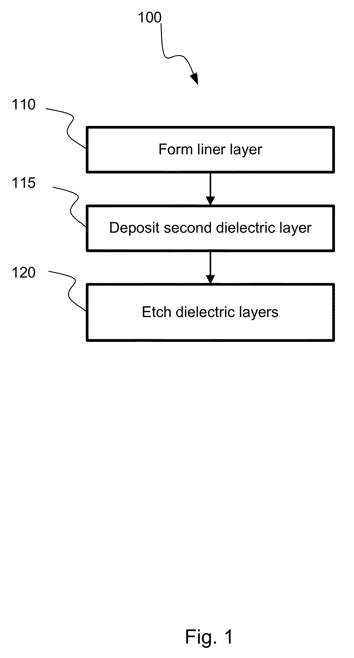
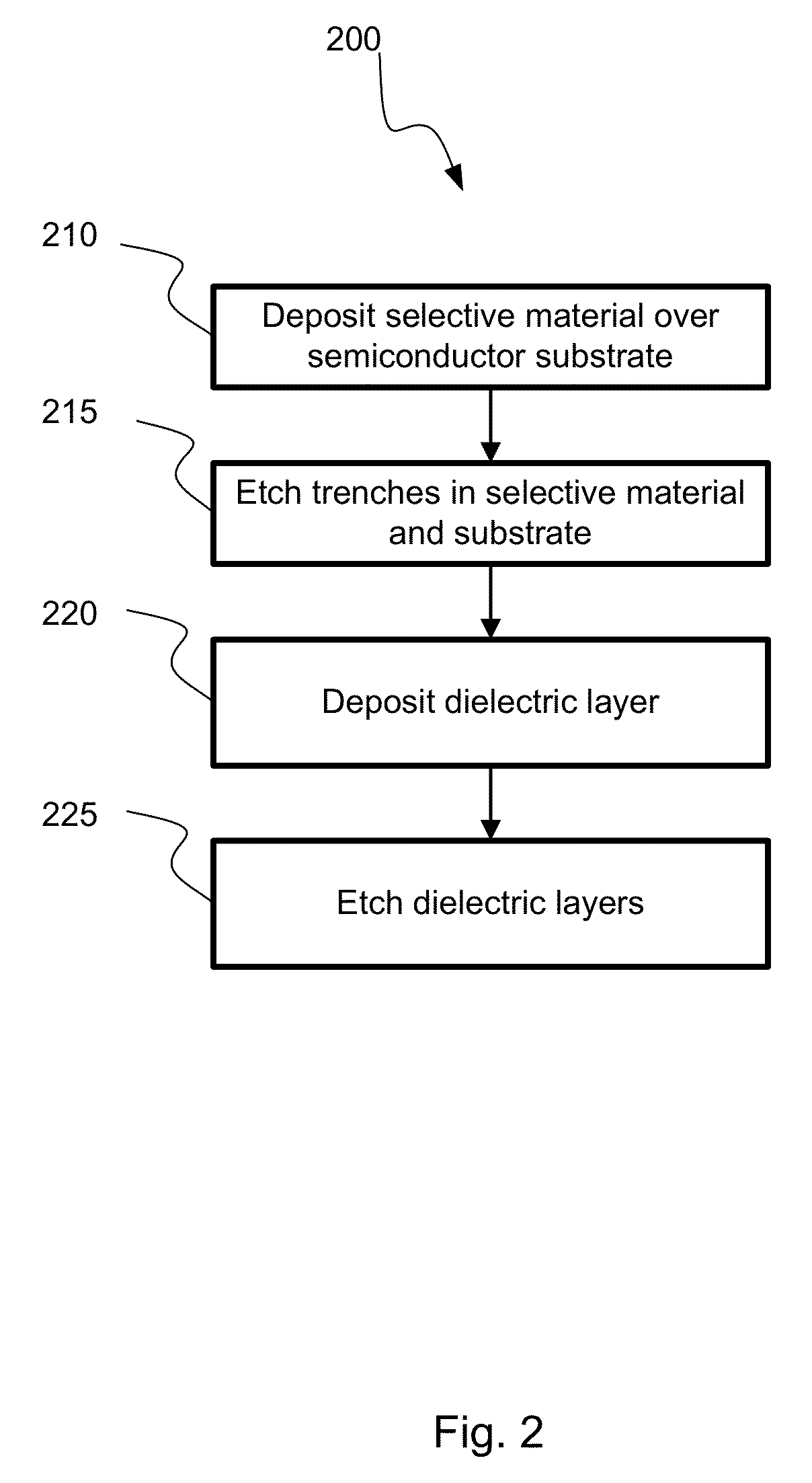
Intrench profile
a technology of intrench and profile, applied in the field of intrench profile, can solve the problems of inability to use wet removal for sti recessing, difficult film removal, and inability to provide the selective removal necessary for such intricate details
- Summary
- Abstract
- Description
- Claims
- Application Information
AI Technical Summary
Benefits of technology
Problems solved by technology
Method used
Image

Examples
examples
[0047]Comparative examples were made between etch selectivity using an etchant gas mixture with and without ammonia. The etches were conducted on a trench that was first lined with an HDP liner layer and then filled with a flowable oxide. The dielectrics were exposed to dry etchant gas mixtures containing nitrogen trifluoride and molecular hydrogen. In one example, the dry etchant gas also contained ammonia, while in a comparative example the dry etchant gas was substantially free of ammonia. As can be seen in Table I below, the dry etchant gas containing ammonia removes more of the flowable oxide in comparison to an HDP oxide than does the dry etchant gas that is substantially free of ammonia:
[0048]
TABLE IETCH DEPTH OF DRY ETCHANT GASSelectivity ofHDP OxideFlowable OxideEtching of FlowableEtch DepthEtch DepthOxide with respect(angstrom)(angstrom)to HDP oxideDry Etchant Gas1141341.19ContainingAmmoniaDry Etchant Gas1141231.09SubstantiallyFree of Ammonia
[0049]FIGS. 4A and 4B show comp...
PUM
| Property | Measurement | Unit |
|---|---|---|
| temperature | aaaaa | aaaaa |
| temperature | aaaaa | aaaaa |
| temperature | aaaaa | aaaaa |
Abstract
Description
Claims
Application Information