Semiconductor device and manufacturing method thereof

a technology of semiconductor devices and manufacturing methods, applied in the direction of semiconductor devices, transistors, electrical devices, etc., can solve the problems of reducing the reliability of a semiconductor device which includes the transistor, and achieve the effects of reducing the oxygen vacancies improving reliability, and reducing the concentration of hydrogen in the oxide semiconductor film

Inactive Publication Date: 2015-01-06
SEMICON ENERGY LAB CO LTD
View PDF127 Cites 13 Cited by
  • Summary
  • Abstract
  • Description
  • Claims
  • Application Information

AI Technical Summary

Benefits of technology

[0011]By performing heat treatment on the oxide semiconductor film at 450° C. or higher, hydrogen concentration can be significantly reduced; however, oxygen vacancies in the oxide semiconductor film are increased at the same time.
[0030]When impurity levels due to hydrogen and defect levels due to oxygen vacancies are reduced, a semiconductor device which includes a transistor using the oxide semiconductor film can have improved reliability.

Problems solved by technology

Change in electrical characteristics (e.g., threshold voltage) which results from operation of a transistor causes a reduction in reliability of a semiconductor device which includes the transistor.

Method used


Image

  • Semiconductor device and manufacturing method thereof
  • Semiconductor device and manufacturing method thereof
  • Semiconductor device and manufacturing method thereof

Examples


embodiment 1

[0055]In this embodiment, a transistor according to one embodiment of the present invention and a method for manufacturing the transistor will be described with reference to FIGS. 1A to 1C, FIGS. 2A to 2C, and FIGS. 3A to 3C.

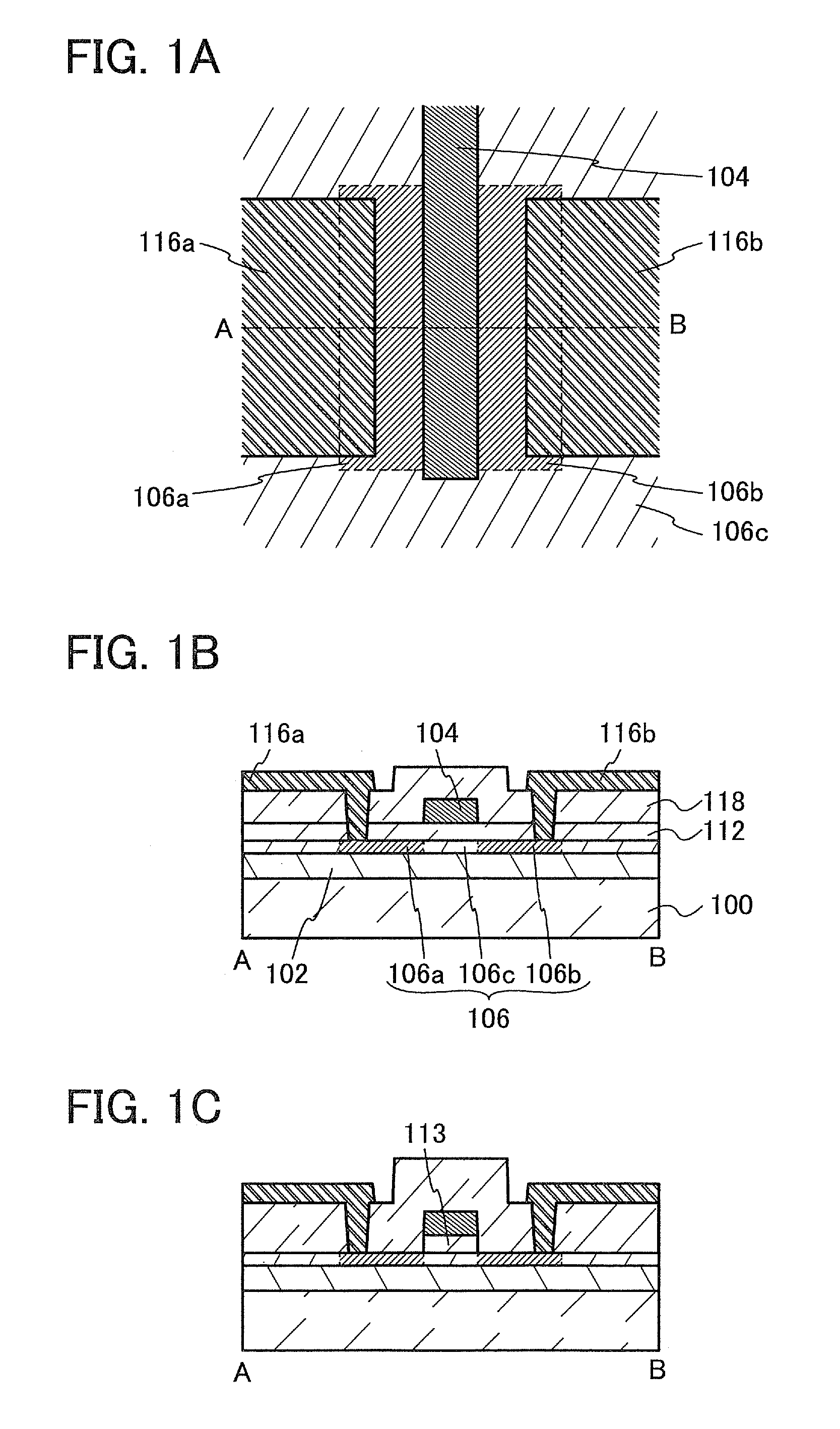
[0056]FIG. 1A is a top view of a transistor according to one embodiment of the present invention. FIG. 1B is a cross-sectional view along dashed-dotted line A-B in FIG. 1A. Note that for simplicity, an interlayer insulating film 118, a gate insulating film 112, and the like are not shown in FIG. 1A.

[0057]The transistor illustrated in FIG. 1B includes a base insulating film 102 formed over a substrate 100; an oxide semiconductor film 106 formed over the base insulating film 102 and including a first region 106a, a second region 106b, and a third region 106c; the gate insulating film 112 formed over the oxide semiconductor film 106; and a gate electrode 104 overlapping with part of the third region 106c of the oxide semiconductor film 106 with the gate insulating ...

embodiment 2

[0128]In this embodiment, transistors having structures different from those of the transistors in Embodiment 1 and a method for manufacturing the transistors will be described with reference to FIGS. 4A to 4C, FIGS. 5A to 5C, FIGS. 6A to 6C, FIGS. 7A to 7C, and FIGS. 8A to 8C.

[0129]FIG. 4A is a top view of a transistor according to one embodiment of the present invention. FIG. 4B is a cross-sectional view along dashed-dotted line A-B in FIG. 4A. Note that for simplicity, an interlayer insulating film 218, a gate insulating film 212, and the like are not shown in FIG. 4A.

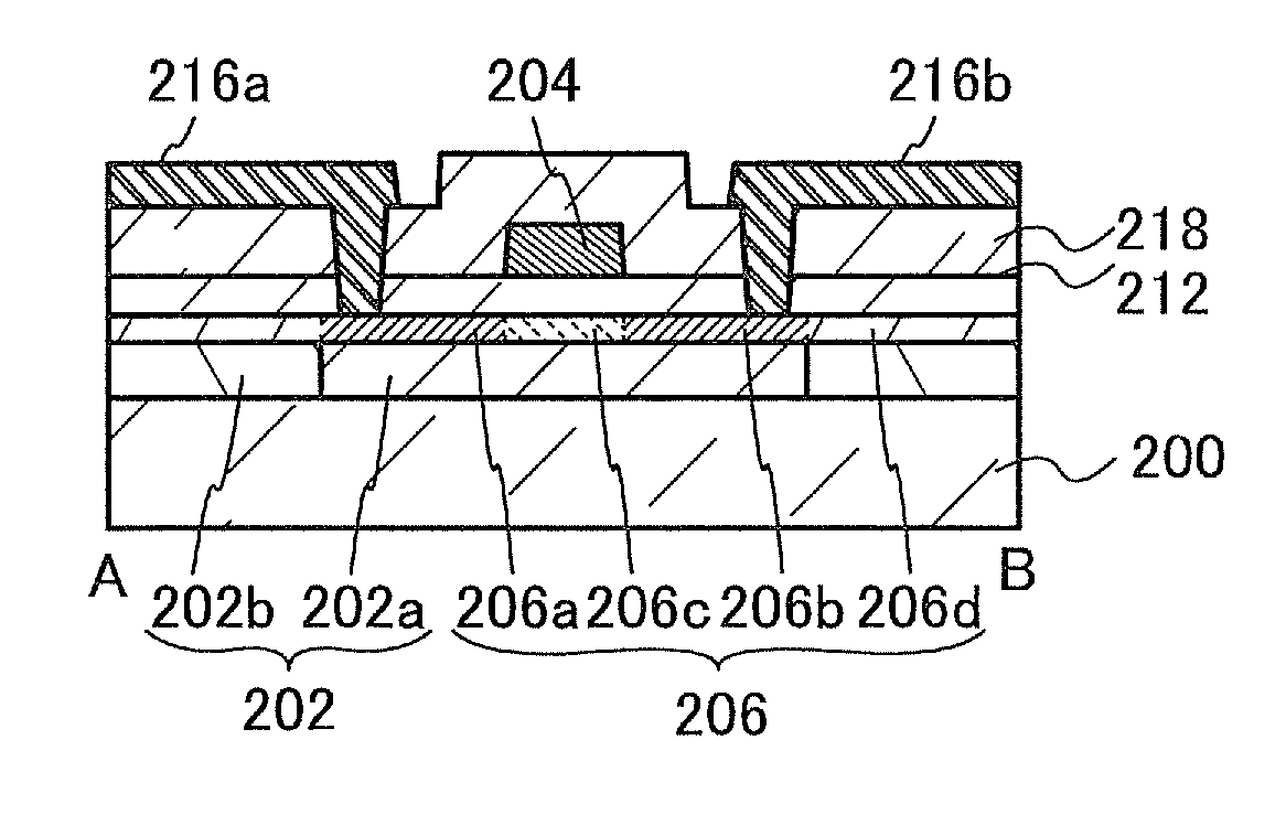
[0130]The transistor illustrated in FIG. 4B includes a base insulating film 202 formed over a substrate 200 and including a first region 202a and a second region 202b; an oxide semiconductor film 206 formed over the base insulating film 202 and including a third region 206a, a fourth region 206b, a fifth region 206c, and a sixth region 206d; the gate insulating film 212 formed over the oxide semiconductor film 206; ...

embodiment 3

[0188]In this embodiment, transistors having structures different from those of the transistors in Embodiments 1 and 2 and a method for manufacturing the transistors will be described with reference to FIGS. 9A and 9B and FIGS. 10A to 10C.

[0189]FIG. 9A is a top view of a transistor according to one embodiment of the present invention. FIG. 9B is a cross-sectional view along dashed-dotted line A-B in FIG. 9A. Note that for simplicity, a gate insulating film 312 and the like are not shown in FIG. 9A.

[0190]The transistor illustrated in FIG. 9B includes a base insulating film 302 over a substrate 300; an oxide semiconductor film 306 formed over the base insulating film 302; an electrode 316a and an electrode 316b formed over the oxide semiconductor film 306 and electrically isolated from each other; the gate insulating film 312 over the oxide semiconductor film 306, the electrode 316a, and the electrode 316b; and a gate electrode 304 provided over the gate insulating film 312 to overlap...


PUM


Abstract

Hydrogen concentration and oxygen vacancies in an oxide semiconductor film are reduced. Reliability of a semiconductor device which includes a transistor using an oxide semiconductor film is improved. One embodiment of the present invention is a semiconductor device which includes a base insulating film; an oxide semiconductor film formed over the base insulating film; a gate insulating film formed over the oxide semiconductor film; and a gate electrode overlapping with the oxide semiconductor film with the gate insulating film provided therebetween. The base insulating film shows a signal at a g value of 2.01 by electron spin resonance. The oxide semiconductor film does not show a signal at a g value of 1.93 by electron spin resonance.

Description

BACKGROUND OF THE INVENTION[0001]1. Field of the Invention[0002]The present invention relates to a semiconductor device and a manufacturing method thereof.[0003]Note that in this specification, a semiconductor device refers to any device that can function by utilizing semiconductor characteristics, and an electro-optical device, a semiconductor circuit, an electronic device, and the like are all semiconductor devices.[0004]2. Description of the Related Art[0005]A technique for forming a transistor by using a semiconductor film formed over a substrate having an insulating surface has attracted attention. The transistor is applied to a wide range of semiconductor devices such as an integrated circuit (IC) and an image display device (display device). A silicon-based semiconductor is widely known as a semiconductor applicable to the transistor. In recent years, an oxide semiconductor has attracted attention.[0006]For example, a transistor in which an amorphous oxide film containing ind...

Claims


Application Information

Patent Timeline
Patent Type & Authority Patents(United States)
IPC IPC(8): H01L21/477H01L29/786
CPCH01L29/7869H01L29/66742H01L29/78603H01L29/42364
Inventor SASAKI, TOSHINARINODA, KOSEISATO, YUHEIENDO, YUTA
Owner SEMICON ENERGY LAB CO LTD
Why Eureka
Try Eureka