Semiconductor device and method for manufacturing the same

a technology of semiconductor devices and semiconductor films, which is applied in the direction of semiconductor devices, basic electric elements, electrical equipment, etc., can solve the problems of reducing the reliability of the semiconductor device, not enough to reduce the hydrogen concentration of the gate insulating film, etc., and achieves excellent gate insulating film and stable electric characteristics.

Active Publication Date: 2013-02-28
SEMICON ENERGY LAB CO LTD
View PDF6 Cites 14 Cited by
  • Summary
  • Abstract
  • Description
  • Claims
  • Application Information

AI Technical Summary

Benefits of technology

[0038]A semiconductor device including an oxide semiconductor and having stable electric characteristics can be provided. A semiconductor device including an oxide semiconductor and an excellent gate insulating film can be provided. Further, a method for manufacturing the semiconductor device can be provided.

Problems solved by technology

However, it is not enough to reduce hydrogen concentration of the gate insulating film on the side in contact with the interface with the oxide semiconductor film because when oxygen deficiency in the oxide semiconductor film are combined with hydrogen or the like which remains in the gate insulating film, electrons (carriers) are generated in the film.
Hydrogen or the like which remains in the gate insulating film changes the electrical characteristics of the transistor including the oxide semiconductor film, which leads to a reduction in reliability of the semiconductor device.

Method used


Image

  • Semiconductor device and method for manufacturing the same
  • Semiconductor device and method for manufacturing the same
  • Semiconductor device and method for manufacturing the same

Examples


embodiment 1

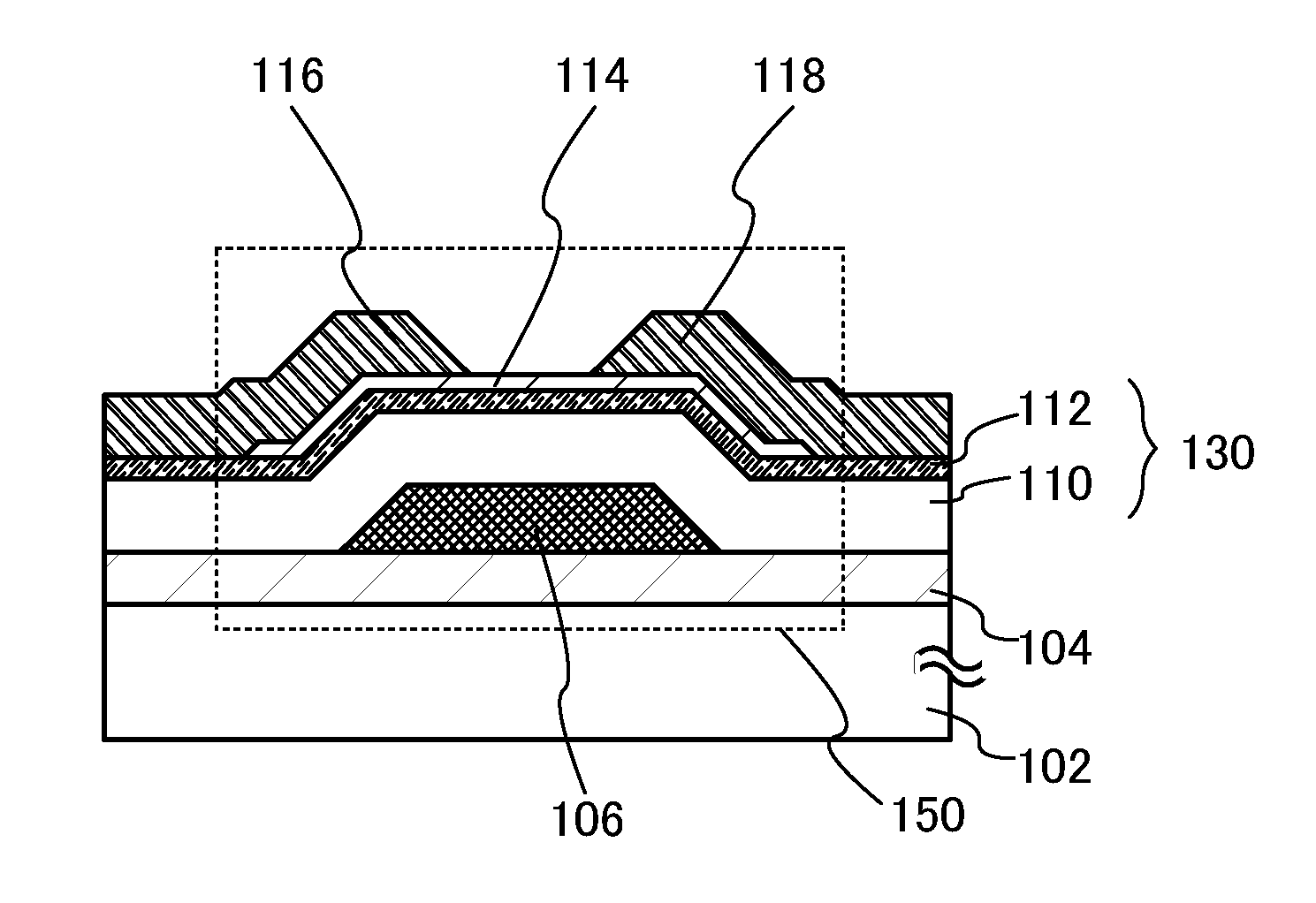
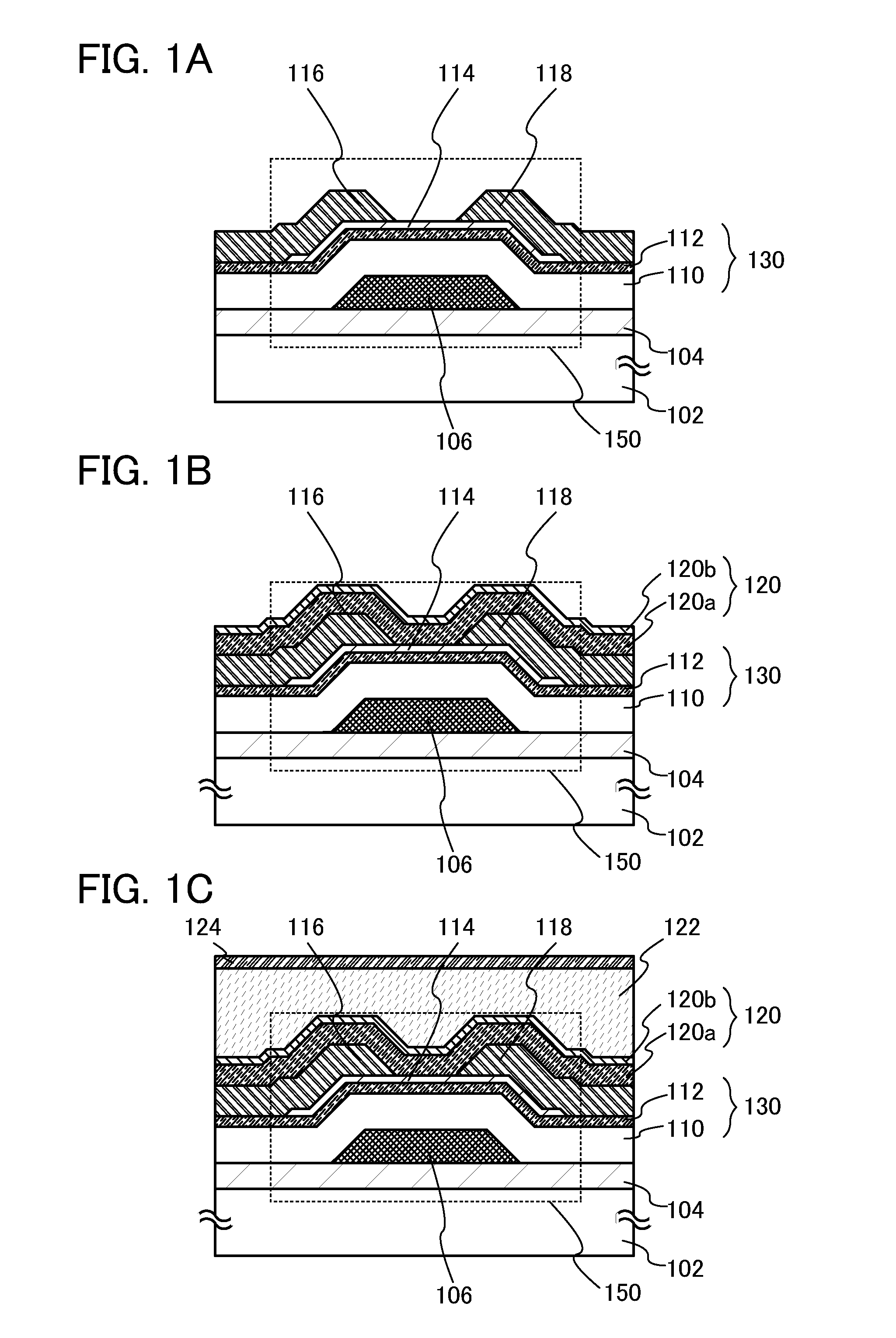
[0061]In this embodiment, a mode of a semiconductor device according to the present invention is described with reference to FIGS. 1A to 1C. FIGS. 1A to 1C each show a cross-sectional view of a semiconductor device including an oxide semiconductor film.

[0062]A semiconductor device in FIG. 1A includes a substrate 102, a base insulating film 104 over the substrate 102, a gate electrode 106 over the base insulating film 104, a silicon oxynitride film 110 over the base insulating film 104 and the gate electrode 106, an oxygen release type oxide film 112 and which is formed over the silicon oxynitride film 110, an oxide semiconductor film 114 over the oxygen release type oxide film 112, a source electrode 116 over the oxygen release type oxide film 112 and the oxide semiconductor film 114, and a drain electrode 118 over the oxygen release type oxide film 112 and the oxide semiconductor film 114.

[0063]In the semiconductor device in FIG. 1A, a gate insulating film 130 includes the silicon ...

embodiment 2

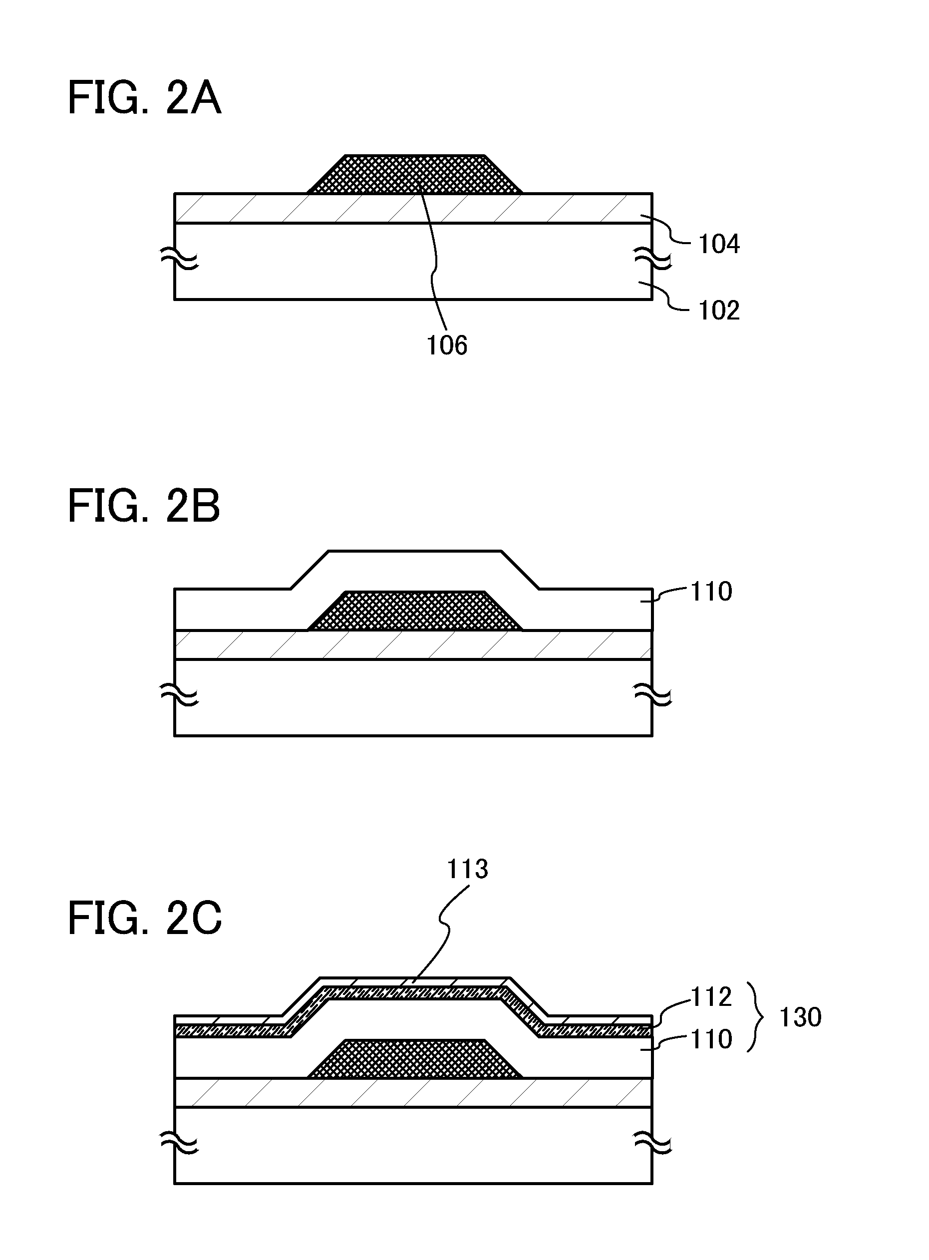
[0093]In this embodiment, methods for manufacturing the semiconductor devices in FIGS. 1A to 1C in Embodiment 1 are described with reference to FIGS. 2A to 2C, FIGS. 3A to 3C, and FIGS. 4A and 4B. Note that portions similar to those in FIGS. 1A to 1C are denoted by the same reference numerals, and description thereof is skipped.

[0094]First, the base insulating film 104 is formed over the substrate 102. Then, the gate electrode 106 is formed over the base insulating film 104 (see FIG. 2A).

[0095]As the substrate 102, a substrate of a glass material such as aluminosilicate glass, aluminoborosilicate glass, or barium borosilicate glass is used. In the mass production, a mother glass with the following size is preferably used for the substrate 102: the 8-th generation (2160 mm×2460 mm); the 9-th generation (2400 mm×2800 mm, or 2450 mm×3050 mm); the 10-th generation (2950 mm×3400 mm); or the like. High process temperature and a long period of process time drastically shrink the mother gla...

embodiment 3

[0172]In this embodiment, a modification example of the semiconductor device in FIG. 1C of Embodiment 1 is described with reference to FIGS. 5A to 5C. Note that portions similar to those in FIGS. 1A to 1C are denoted by the same reference numerals, and a description thereof is skipped.

[0173]The semiconductor device in FIG. 5C is an example of this embodiment. FIGS. 5A and 5B illustrate a method for manufacturing the semiconductor device in FIG. 5C.

[0174]A semiconductor device in FIG. 5C includes the substrate 102, the base insulating film 104 over the substrate 102, the gate electrode 106 over the base insulating film 104, the silicon oxynitride film 110 over the base insulating film 104 and the gate electrode 106, the oxygen release type oxide film 112 and which is formed over the silicon oxynitride film 110, the oxide semiconductor film 114 over the oxygen release type oxide film 112, the source electrode 116 over the oxygen release type oxide film 112 and the oxide semiconductor ...


PUM


Abstract

Provided is a semiconductor device including an oxide semiconductor and having stable electrical characteristics. Specifically, a semiconductor device including an oxide semiconductor and including a gate insulating film with favorable characteristics is provided. Further, a method for manufacturing the semiconductor device is provided. The semiconductor device includes a gate electrode, a gate insulating film over the gate electrode, an oxide semiconductor film over the gate insulating film, and a source electrode and a drain electrode in contact with the oxide semiconductor film. The gate insulating film includes at least a silicon oxynitride film and an oxygen release type oxide film which is formed over the silicon oxynitride film. The oxide semiconductor film is formed on and in contact with the oxygen release type oxide film.

Description

BACKGROUND OF THE INVENTION[0001]1. Field of the Invention[0002]The present invention relates to a semiconductor device and a method for manufacturing the semiconductor device.[0003]In this specification, a semiconductor device generally means a device which can function by utilizing semiconductor characteristics, and an electrooptic device, a semiconductor circuit, and electronic equipment are all semiconductor devices.[0004]2. Description of the Related Art[0005]A technique by which transistors are formed using semiconductor thin films formed over a substrate having an insulating surface has been attracting attention. The transistor is applied to a wide range of electronic devices such as an integrated circuit (IC) or an image display device (display device). A silicon-based semiconductor material is widely known as a material for a semiconductor thin film applicable to a transistor. As another material, an oxide semiconductor has been attracting attention.[0006]For example, a tra...

Claims


Application Information

Patent Timeline
Patent Type & Authority Applications(United States)
IPC IPC(8): H01L29/22
CPCH01L29/7869H01L29/4908
Inventor WATANABE, MASAHIROMASHIYAMA, MITSUOHANDA, TAKUYAOKAZAKI, KENICHIYAMAZAKI, SHUNPEI
Owner SEMICON ENERGY LAB CO LTD
Why Eureka
Try Eureka