Field effect transistor and method for manufacturing the same

a field effect transistor and transistor technology, applied in transistors, semiconductor devices, electrical equipment, etc., can solve the problems of insufficient resistance to voltage, method cannot be employed, and hydrogen that remained in this manner cannot be removed or removed in later steps

Inactive Publication Date: 2014-11-25
SEMICON ENERGY LAB CO LTD
View PDF134 Cites 13 Cited by
  • Summary
  • Abstract
  • Description
  • Claims
  • Application Information

AI Technical Summary

Benefits of technology

[0018]An object of one embodiment of the present invention is to provide a method for manufacturing a FET having stable characteristics. Another object is to provide a novel FET having a structure suitable for the above object.
[0022]One embodiment of the present invention provides a method for manufacturing a FET or a structure of a FET in which the hydrogen concentration can be sufficiently reduced even when an insulating film which corresponds to the insulating film 203 is formed by a plasma CVD method.
[0041]By employing any of the above-described structures, at least one of the above-described objects can be achieved. That is, the insulating film can be formed by a CVD method or a sputtering method. According to one embodiment of the present invention, the semiconductor layer or the wiring can be prevented from overlapping with a step portion, so that insufficient insulation due to insufficient step coverage in the step portion can be suppressed.
[0042]In addition, according to one embodiment of the present invention, even when the insulating film is formed by a CVD method, oxygen diffuses from the oxide insulating layer formed over the insulating film by heat treatment at 200° C. or higher, so that hydrogen existing in the insulating film can be oxidized to be fixed as water or released as water from the insulating film. Accordingly, the hydrogen concentration in the insulating film can be sufficiently reduced.

Problems solved by technology

The present inventor assumed that a problem of the method illustrated in FIGS. 4A to 4D was that hydrogen that remained in that manner was not removed or could not be removed in later steps.
In order to reduce the concentration of the hydrogen to a sufficiently low concentration, treatment at considerably high temperatures has been necessary; however, when heat resistance of the substrate 201 or the wirings 202a and 202b is not high enough, such a method cannot be employed.
On the other hand, when the insulating film 203 is formed by a sputtering method by which the hydrogen concentration can be sufficiently reduced, there is another problem in that the withstand voltage is insufficient because of the above-described problem of step coverage.

Method used


Image

  • Field effect transistor and method for manufacturing the same
  • Field effect transistor and method for manufacturing the same
  • Field effect transistor and method for manufacturing the same

Examples


embodiment 1

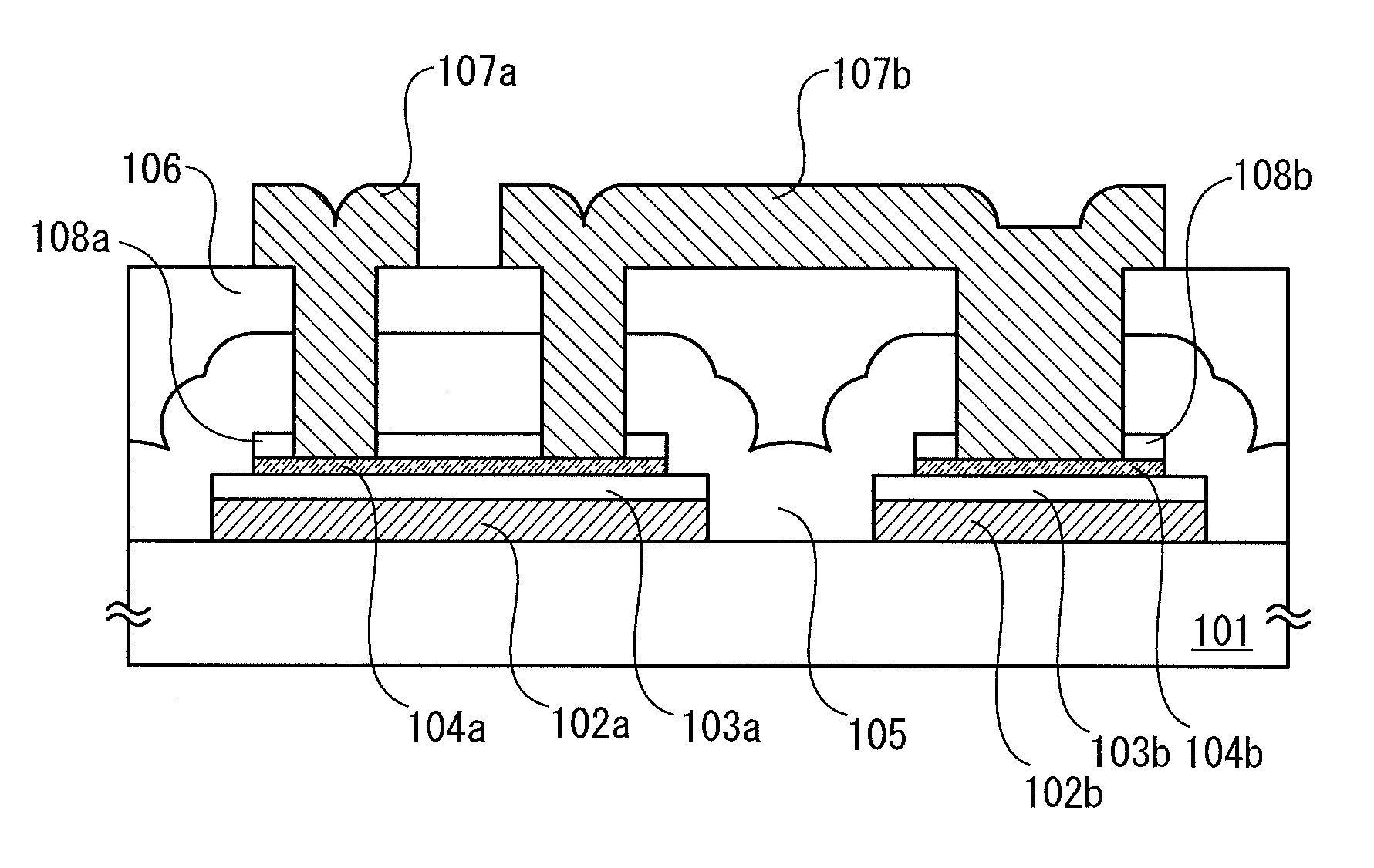
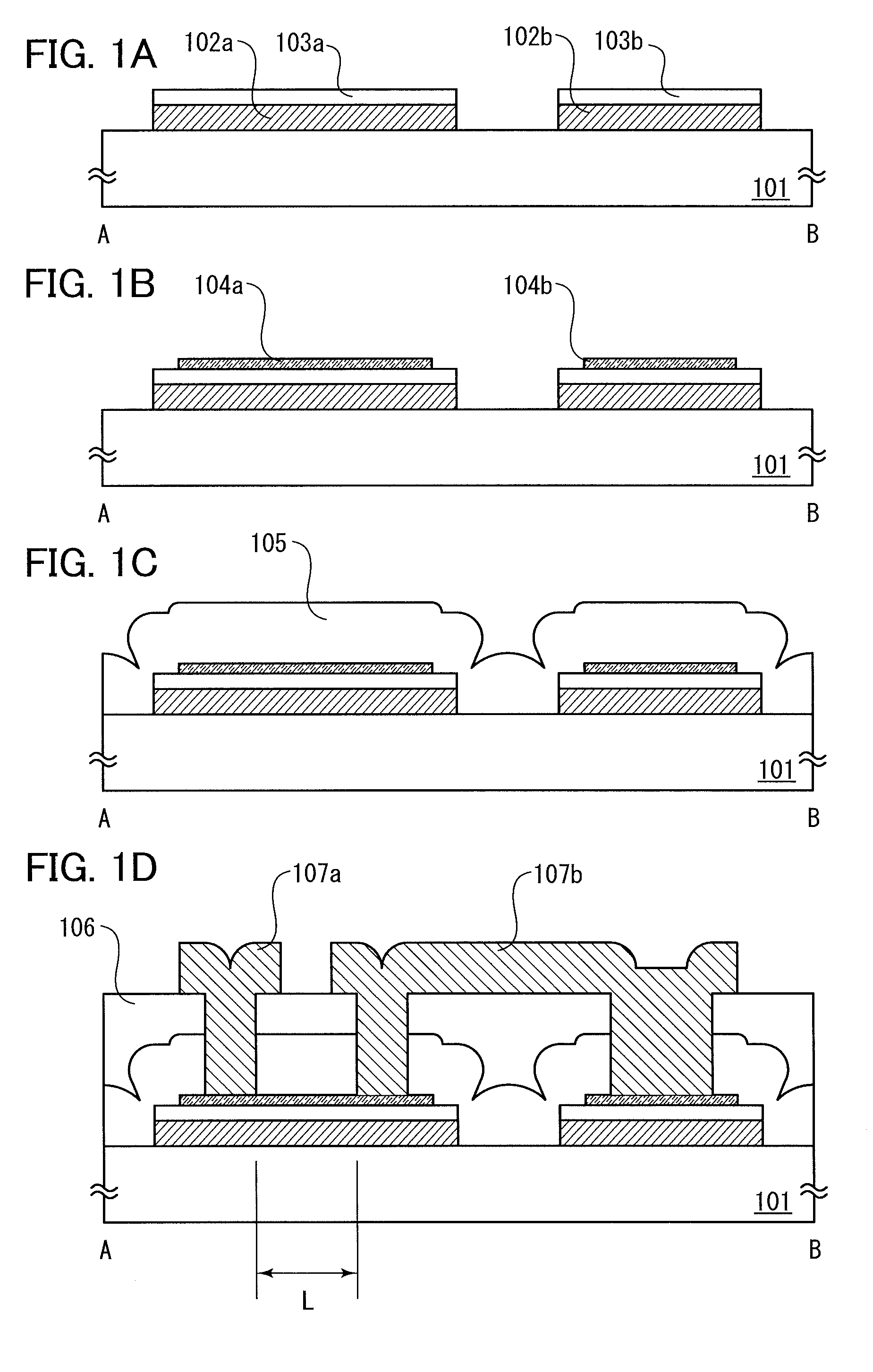
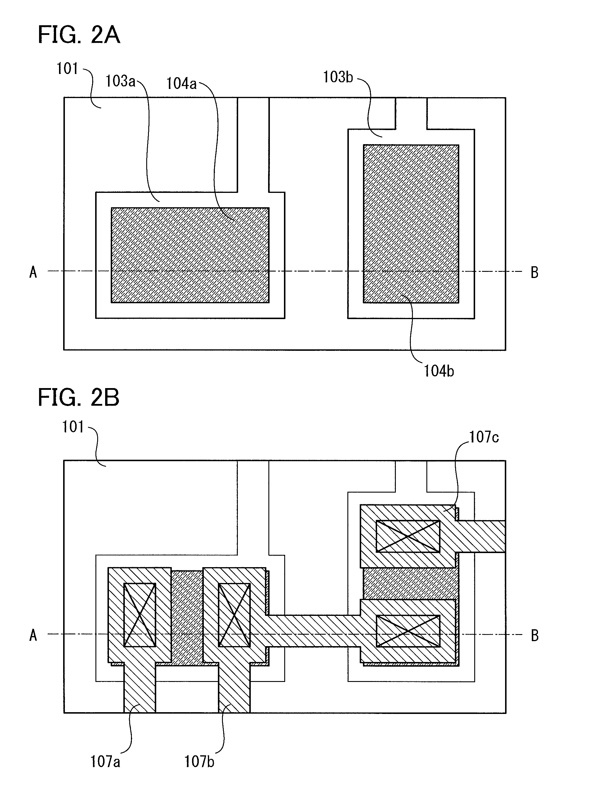
[0053]FIGS. 1A to 1D illustrate cross-sectional views of processes for manufacturing a FET which is one embodiment of the present invention and FIGS. 2A and 2B illustrate top views of the processes for manufacturing the FET which is one embodiment of the present invention. FIGS. 1A to 1D are cross sections along line A-B in FIGS. 2A and 2B.

[0054]First, a conductive layer and an insulating film are formed over a substrate 101. The conductive layer and the insulating film can be formed by applying any deposition method; however, it is preferable that a deposition method such as a sputtering method, a CVD method, or a laser ablation method, which is performed in a state where an atmosphere is sufficiently managed, be employed and that the insulating film be formed without exposure of the conductive layer to the air after formation of the conductive layer.

[0055]The conductive layer can be formed using any kind of materials. For example, for the conductive layer, any kind of metals such ...

embodiment 2

[0097]In this embodiment, an example of a FET having a structure different from that described in Embodiment 1 will be described. FETs illustrated in FIGS. 3A and 3B are each the same as the FET illustrated in FIG. 1D in that the FETs include, over the substrate 101, the wirings 102a and 102b each of which functions as a gate electrode; the insulating film 103a which is provided over the wiring 102a, has substantially the same shape as the wiring 102a, and functions as a gate insulating film; the insulating film 103b which is provided over the wiring 102b, has substantially the same shape as the wiring 102b, and functions as a gate insulating film; the semiconductor layer 104a which is provided over the insulating film 103a and whose edge is placed inside the edge of the insulating film 103a; the semiconductor layer 104b which is provided over the insulating film 103b and whose edge is placed inside the edge of the insulating film 103b; the oxide insulating layer 105; the planarizat...

embodiment 3

[0110]In this embodiment, an example of a FET having a structure different from those in Embodiments 1 and 2 and an active-matrix circuit including the FET will be described. An active-matrix circuit is a circuit in which unit circuits illustrated in FIG. 5A are arranged in matrix. The circuit in FIG. 5A is used in display devices in which grayscales are controlled by voltage, such as liquid crystal display devices. Note that in addition to the circuit in FIG. 5A, there are active-matrix circuits used for display devices in which grayscales are controlled by current, such as some electroluminescent display devices.

[0111]The circuit illustrated in FIG. 5A includes a FET 301 as a switching element; a display element 302 including a first electrode and a second electrode which face each other; a storage capacitor 303 including a first electrode and a second electrode which face each other; a scan line 304 which transmits a signal for selecting the FET 301; a data line 305 which transmi...


PUM


Abstract

Provided is a novel structure of a field effect transistor using a metal-semiconductor junction. The field effect transistor includes a wiring which is provided over a substrate and also functions as a gate electrode; an insulating film which is provided over the wiring, has substantially the same shape as the wiring, and also functions as a gate insulating film; a semiconductor layer which is provided over the insulating film and includes an oxide semiconductor and the like; an oxide insulating layer which is provided over the semiconductor layer and whose thickness is 5 times or more as large as the sum of the thickness of the insulating film and the thickness of the semiconductor layer or 100 nm or more; and wirings which are connected to the semiconductor layer through openings provided in the oxide insulating layer.

Description

BACKGROUND OF THE INVENTION[0001]1. Field of the Invention[0002]The present invention relates to a field effect transistor (FET) including a semiconductor.[0003]2. Description of the Related Art[0004]In a field effect transistor (hereinafter referred to as a FET), regions called a source and a drain are provided in a semiconductor. Voltage is applied to the semiconductor from a region called a gate through an insulating film or a Schottky barrier in the state where voltage is applied between the source and the drain, so that the state of the semiconductor is controlled; thus, current flowing between the source and the drain is controlled. As the semiconductor, an element such as silicon or germanium, a compound such as gallium arsenide, indium phosphide, gallium nitride, zinc sulfide, or cadmium telluride, or the like can be used.[0005]In recent years, FETs including an oxide such as zinc oxide or an indium gallium zinc oxide-based compound as the semiconductor have been reported (P...

Claims


Application Information

Patent Timeline
Patent Type & Authority Patents(United States)
IPC IPC(8): H01L29/786H01L21/00H01L27/12H01L29/24H01L27/13
CPCH01L27/13H01L27/1255H01L27/1225H01L29/242H01L29/7869H01L21/02614H01L21/385H01L21/02266H01L29/66969H01L21/477H01L21/02565
Inventor TAKEMURA, YASUHIKO
Owner SEMICON ENERGY LAB CO LTD
Why Eureka
Try Eureka