Method for manufacturing oxide semiconductor film and method for manufacturing semiconductor device

a semiconductor film and manufacturing method technology, applied in semiconductor devices, vacuum evaporation coatings, coatings, etc., can solve the problems of not being able to use turbo molecular pumps, the composition of oxide semiconductors cannot be easily controlled, etc., and achieve and the reduction of the concentration of hydrogen and the concentration of hydride in the oxide semiconductor film

Active Publication Date: 2011-03-24
SEMICON ENERGY LAB CO LTD
View PDF86 Cites 14 Cited by
  • Summary
  • Abstract
  • Description
  • Claims
  • Application Information

AI Technical Summary

Benefits of technology

[0020]When the oxide semiconductor film is formed, an entrapment vacuum pump is preferably used for evacuating the treatment chamber. For example, a cryopump, an ion pump, or a titanium sublimation pump is preferably used. The vacuum pump such as a turbo molecular pump which evacuates gas by rotating a turbine blade at high speed has characteristics in that the pumping speed with respect to a light gas such as hydrogen is decreased. Therefore, it is not suitable to use a turbo molecular pump for sufficiently evacuating remaining hydrogen and moisture from the treatment chamber of a sputtering apparatus for manufacture of a highly purified oxide semiconductor film. On the other hand, since an entrapment vacuum pump sufficiently evacuates even a light gas such as hydrogen, it is possible to reduce the concentration of hydrogen in the oxide semiconductor film to 5×10¹⁹ / cm3 or less by removal of remaining hydrogen and moisture in the treatment chamber of the sputtering apparatus.
[0029]When the oxide semiconductor film is formed, remaining moisture in a reaction atmosphere is removed; thus, the concentration of hydrogen and the concentration of hydride in the oxide semiconductor film can be reduced. Thus, the oxide semiconductor film can be stabilized.
[0030]When the oxide semiconductor film serving as a channel formation region is formed over the gate insulating film, remaining moisture in a reaction atmosphere is removed; thus, the concentration of hydrogen and the concentration of hydride in the oxide semiconductor film can be reduced. By provision of the silicon oxide film including a defect in contact with the oxide semiconductor film, hydrogen and moisture in the oxide semiconductor film can be diffused into the silicon oxide film, so that the concentration of hydrogen and the concentration of hydride in the oxide semiconductor film can be reduced.
[0031]In addition, the silicon nitride film is formed over the silicon oxide film including a defect in the state where the substrate is heated; thus, hydrogen and moisture can be diffused from the oxide semiconductor film into the silicon oxide film and a barrier film for prevention of entry of moisture from an outer atmosphere can be provided.

Problems solved by technology

However, because the composition of an oxide semiconductor cannot be easily controlled, a difference from a stoichiometric composition of the oxide semiconductor occurs in a process of forming an oxide semiconductor film.
Therefore, it is not suitable to use a turbo molecular pump for sufficiently evacuating remaining hydrogen and moisture from the treatment chamber of a sputtering apparatus for manufacture of a highly purified oxide semiconductor film.

Method used


Image

  • Method for manufacturing oxide semiconductor film and method for manufacturing semiconductor device
  • Method for manufacturing oxide semiconductor film and method for manufacturing semiconductor device
  • Method for manufacturing oxide semiconductor film and method for manufacturing semiconductor device

Examples


Embodiment Construction

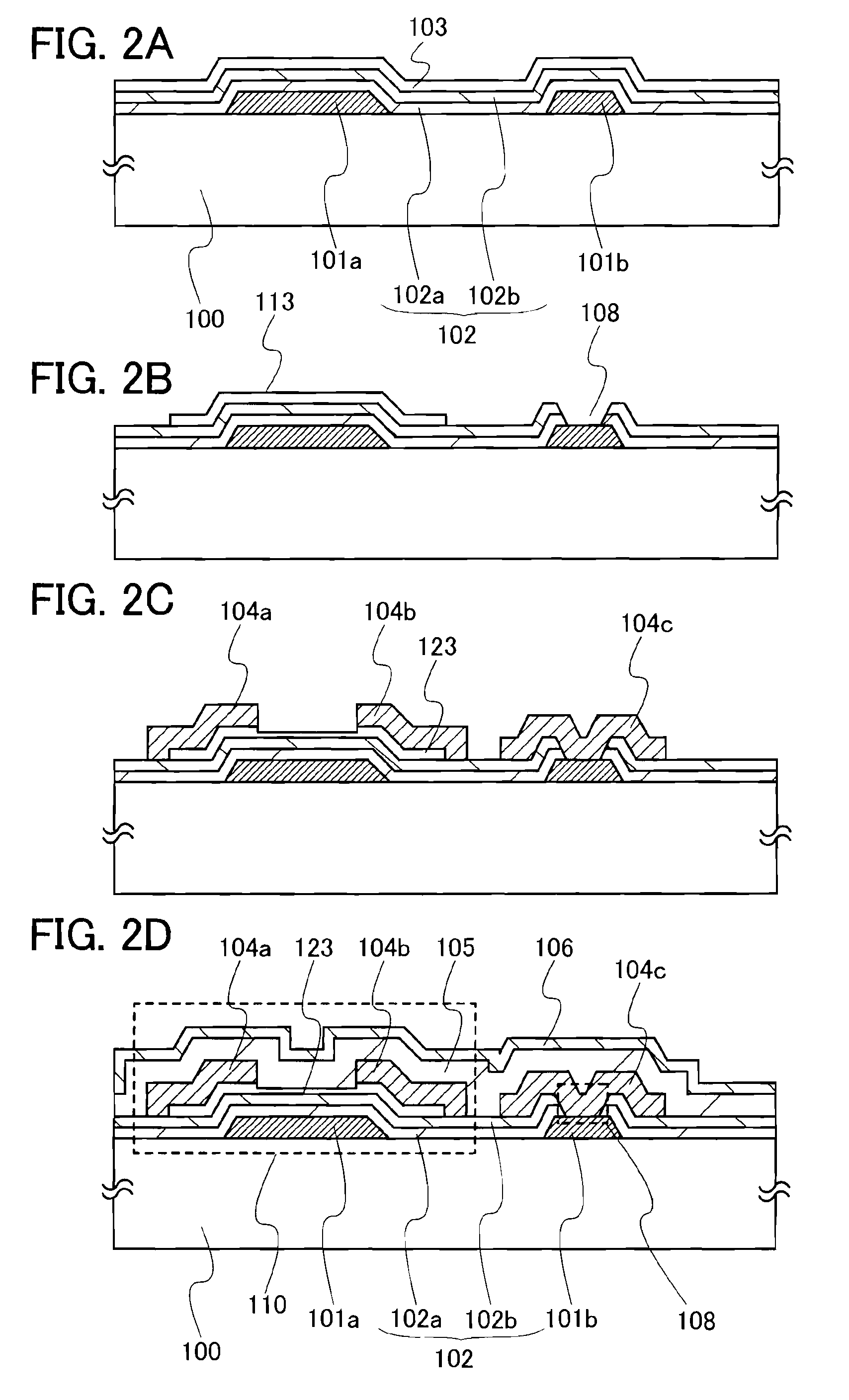
[0037]An embodiment of the disclosed invention will be described. Note that the disclosed invention is not limited to the description below, and it is easily understood by those skilled in the art that a variety of changes and modifications can be made without departing from the spirit and scope of the disclosed invention. Therefore, the disclosed invention should not be interpreted as being limited to the following description of the embodiment.

[0038]In the embodiment described below, the same reference numerals may be used to denote the same components among different drawings. Note that elements in the drawings, that is, the thickness and width of layers, regions, the relative positional relationships between the components, and the like may be exaggerated for the sake of clarity of the description in the embodiment.

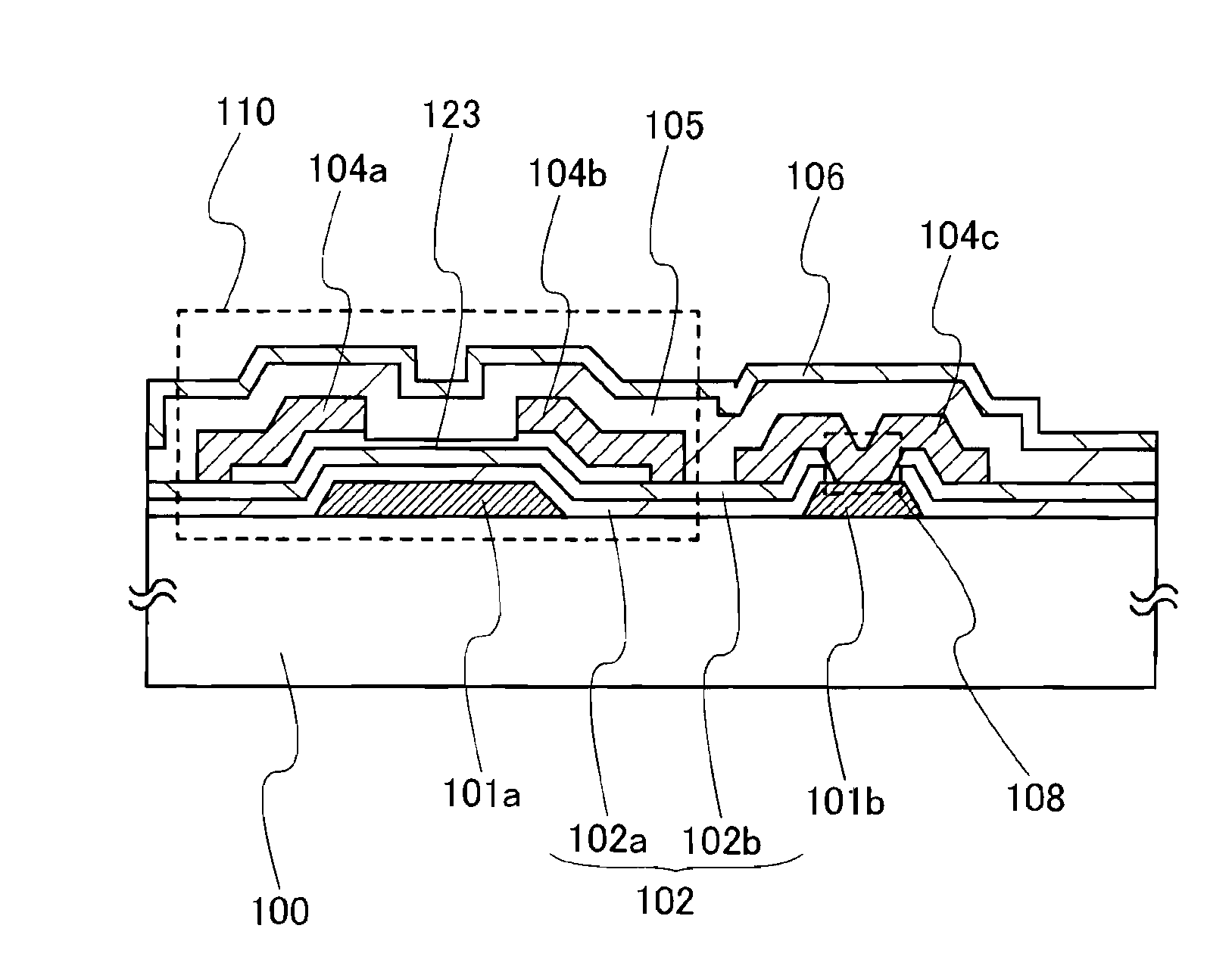
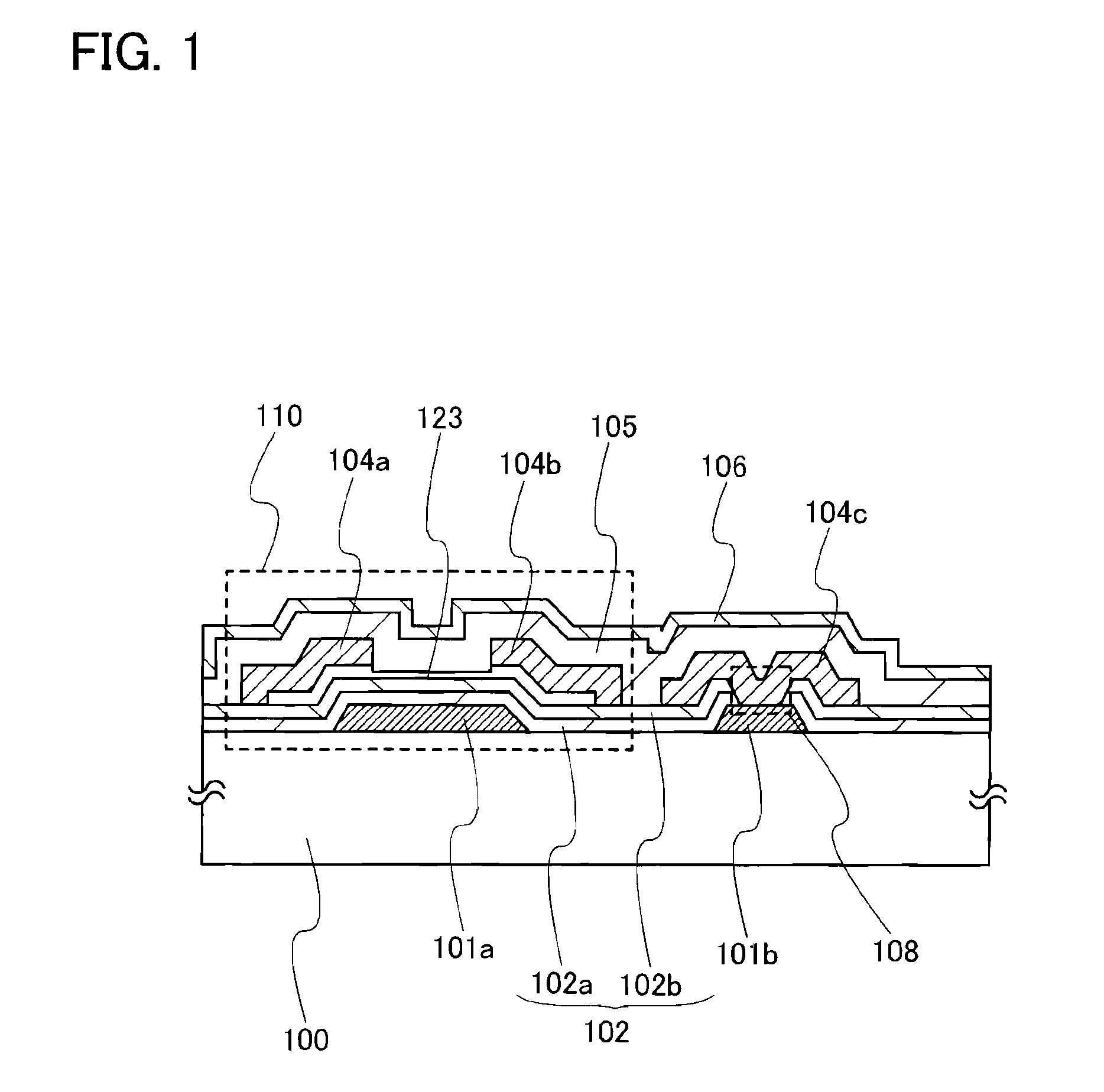
[0039]FIG. 1 illustrates a structure of a semiconductor device. In a thin film transistor 110 of the semiconductor device, a gate electrode 101a and a first wiring 10...


PUM

PropertyMeasurementUnit
temperatureaaaaaaaaaa
thicknessaaaaaaaaaa

Abstract

An object is to provide an oxide semiconductor having stable electric characteristics and a semiconductor device including the oxide semiconductor. A manufacturing method of a semiconductor film by a sputtering method includes the steps of holding a substrate in a treatment chamber which is kept in a reduced-pressure state; heating the substrate at lower than 400° C.; introducing a sputtering gas from which hydrogen and moisture are removed in the state where remaining moisture in the treatment chamber is removed; and forming an oxide semiconductor film over the substrate with use of a metal oxide which is provided in the treatment chamber as a target. When the oxide semiconductor film is formed, remaining moisture in a reaction atmosphere is removed; thus, the concentration of hydrogen and the concentration of hydride in the oxide semiconductor film can be reduced. Thus, the oxide semiconductor film can be stabilized.

Description

TECHNICAL FIELD[0001]One embodiment of the present invention relates to methods for manufacturing an oxide semiconductor film and a semiconductor device using an oxide semiconductor.BACKGROUND ART[0002]A thin film transistor (a TFT) including a semiconductor thin film (having a thickness of several nanometers to several hundreds nanometers) which is formed over a substrate having an insulating surface is applied to a thin film integrated circuit, a liquid crystal display device, or the like. In particular, application of a thin film transistor as a switching element provided in a pixel of a liquid crystal display device is expanding.[0003]In a conventional technique, a thin film transistor is manufactured using a silicon semiconductor. However, in recent years, a technique for manufacturing a thin film transistor using a metal oxide having semiconductor characteristics has attracted attention. Indium oxide is a well-known material as a metal oxide, and has been used as a transparent...

Claims


Application Information

Patent Timeline
Patent Type & Authority Applications(United States)
IPC IPC(8): H01L21/34C23C14/34
CPCC23C14/086H01L21/02422H01L21/02554H01L29/66742H01L21/02631H01L29/7869H01L21/02565
Inventor YAMAZAKI, SHUNPEISAKATA, JUNICHIROMIYANAGA, AKIHARUSAKAKURA, MASAYUKIKOEZUKA, JUNICHIMARUYAMA, TETSUNORIIMOTO, YUKI
Owner SEMICON ENERGY LAB CO LTD
Why Eureka
Try Eureka