

Wiring structure, thin film transistor array substrate including the same, and display device
a technology of thin film transistors and array substrates, applied in semiconductor devices, semiconductor/solid-state device details, instruments, etc., can solve the problems of reducing the yield reducing the reliability of tft array substrates, so as to achieve excellent electrical connection and suppress the occurrence of film floating
- Summary
- Abstract
- Description
- Claims
- Application Information
AI Technical Summary
Benefits of technology
Problems solved by technology
Method used
Image

Examples
Embodiment Construction
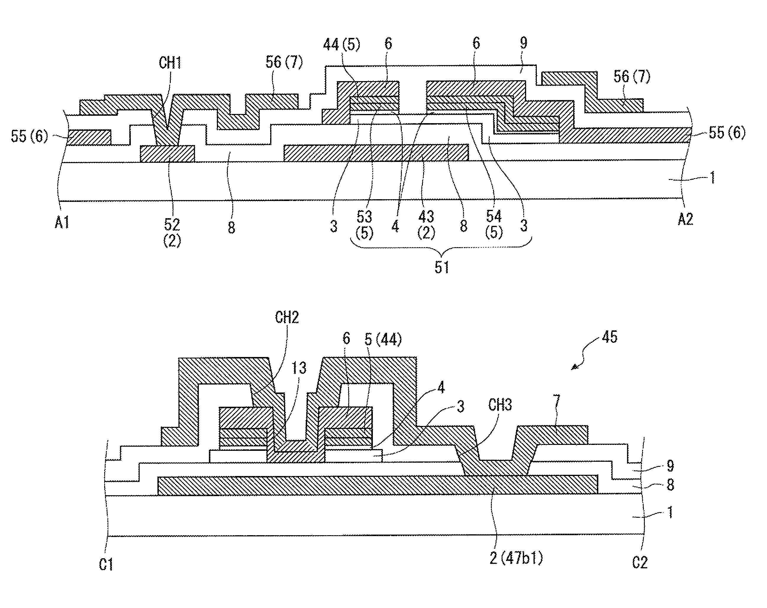
[0035]Preferred embodiments of the present invention will be hereinafter described, but the application of the present invention is not limited thereto. For the convenience of explanation, the description of explanation and the drawings is appropriately omitted or simplified. For example, the drawings are schematically represented, and do not specify precise dimensions and the like of constituent elements shown therein. Additionally, elements denoted by the same reference numerals in respective figures show respective similar elements, and explanation of these elements will not be repeated.
[0036]
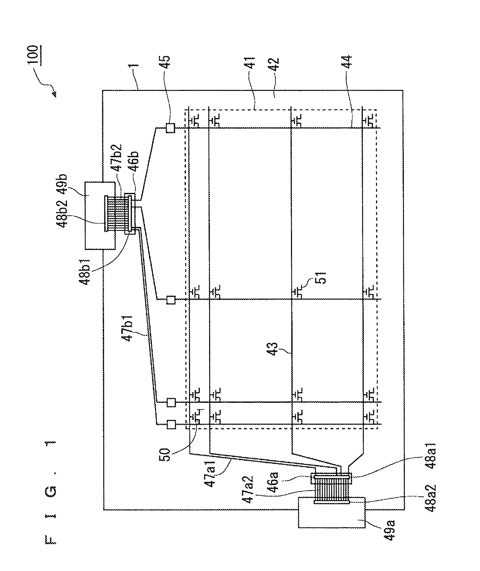
[0037]First, a configuration example of a liquid crystal display device capable of applying a wiring structure according to the present invention is shown. FIG. 1 is a plan view showing a TFT array substrate 100 configuring the liquid crystal display device according to a preferred embodiment of the present invention. As shown in FIG. 1, the TFT array substrate 100 includes pixels 50 serving...
PUM
 Abstract
Description
Claims
Application Information