Surface mountable over-current protection device

a protection device and surface mount technology, applied in the direction of resistor details, resistors, positive temperature coefficient thermistors, etc., can solve the problems of reducing the performance reducing the efficiency of smd over-current protection devices, and often losing the characteristic of voltage endurance of ptc conductive composites, etc., to achieve the effect of effectively dissipating the heat generated by the ptc material layer, increasing heat dissip

Active Publication Date: 2015-01-13
POLYTRONICS TECH
View PDF11 Cites 6 Cited by
  • Summary
  • Abstract
  • Description
  • Claims
  • Application Information

AI Technical Summary

Benefits of technology

[0009]The present application is to provide a surface mountable over-current protection device, in which conductive filler of high conductivity and good heat dissipation structure are utilized. This enables the surface mountable over-current protection device to exhibit excellent resistivity and high hold current.
[0012]In an embodiment, the first or second metal foils may be view as a part of the connecting conductors if they are capable of effectively dissipating the heat generated by the PTC material layer.
[0013]When heat dissipation efficiency increases, the heat of PTC material layer can be transferred to outside more rapidly. Therefore, the temperature incremental rate of the PTC material will be diminished, and as a result the SMD over-current protection device can acquire higher hold current. If the heat dissipation factor is greater than 0.6, the hold current per unit area of the over-current protection device can increase to be greater than 1 A / mm2 due to good heat dissipation efficiency and the use of low resistivity material.

Problems solved by technology

Even though the low resistivity below 0.2 Ω-cm is achieved, the PTC conductive composite often loses the characteristic of voltage endurance.
If carbon black is applied to a surface mountable device (SMD) with fixed covered area, the hold current of the SMD is limited to certain level due to the resistance limitation of carbon black.
Although a multi-layer PTC structure could be used to increase the hold current, SMD over-current protection device performance is eventually limited due to the limitation of total height as well as the number of PTC layers of the SMD device.
However, as the rapid advancement of the mobile communication, the mobile apparatuses are demanded to be lightweight, compact and more powerful.
Therefore, larger operating current is needed and the hold current per PTC area of 1 A / mm2 is not enough for current PTC protection applications.

Method used


Image

  • Surface mountable over-current protection device
  • Surface mountable over-current protection device
  • Surface mountable over-current protection device

Examples


first embodiment

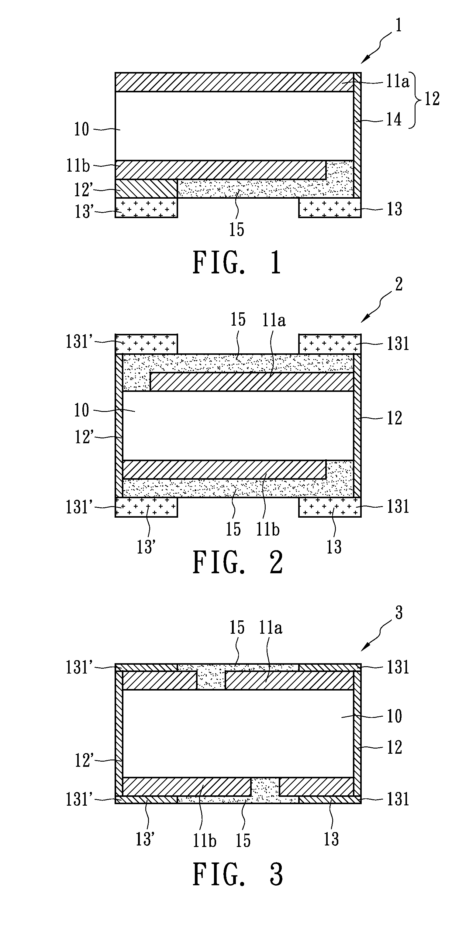
[0029]FIG. 1 illustrates the surface mountable over-current protection device 1, which is suitable to be secured to a substrate (not shown). A first electrode 13 and a second electrode 13′ corresponding to the first electrode 13 are usually located on the same plane. The surface mountable over-current protection device 1 could be designed to contain only one electrode set comprising the first electrode 13 and the second electrode 13′ such that only a specific surface thereof could adhere to the surface of the substrate. The design in FIG. 1 is usually applied to a narrow space and meets the requirements of one-way heat conduction or one-way heat insulation. In this embodiment, the first electrode 13, a conductor 14, a first metal foil 11a, a PTC material layer 10, a second metal foil 11b, a connecting conductor 12′, and the second electrode 13′ form a conductive circuit to connect an external device (not shown) and a power source (not shown). In addition, an insulating layer 15 is d...

third embodiment

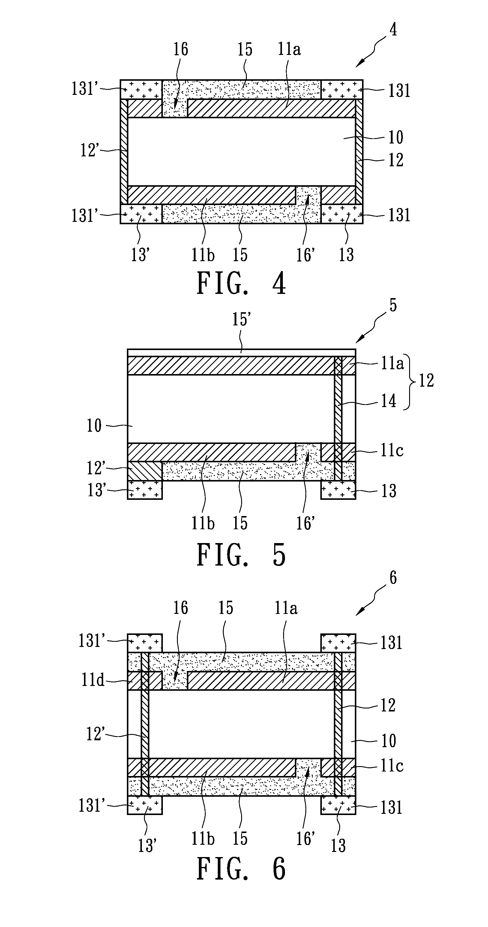
[0031]FIG. 3 illustrates the surface mountable over-current protection device 3, in which the first connecting conductor 12 and the second connecting conductor 12′ are developed by metallic electroplating on sidewall surfaces of the surface mountable over-current protection device 3 to form wrap-around electrical conductors. The first connecting conductor 12 connects the pair of the first electrode layers 131 and the first metal foil 11a, and the second connecting conductor 12′ connects the pair of the second electrode layers 131′ and the second metal foil 11b. The upper first electrode layer 131 contacts the surface of the first metal foil 11a, and the lower second electrode layer 131′ contacts the surface of the second metal foil 11b. In addition, the first and the second connecting conductors 12 and 12′ connecting the first and the second metal foils 11a and 11b and electrodes 13 and 13′ can be formed by soldering, electroplating, and then reflow and heat-curing. In this embodime...

fourth embodiment

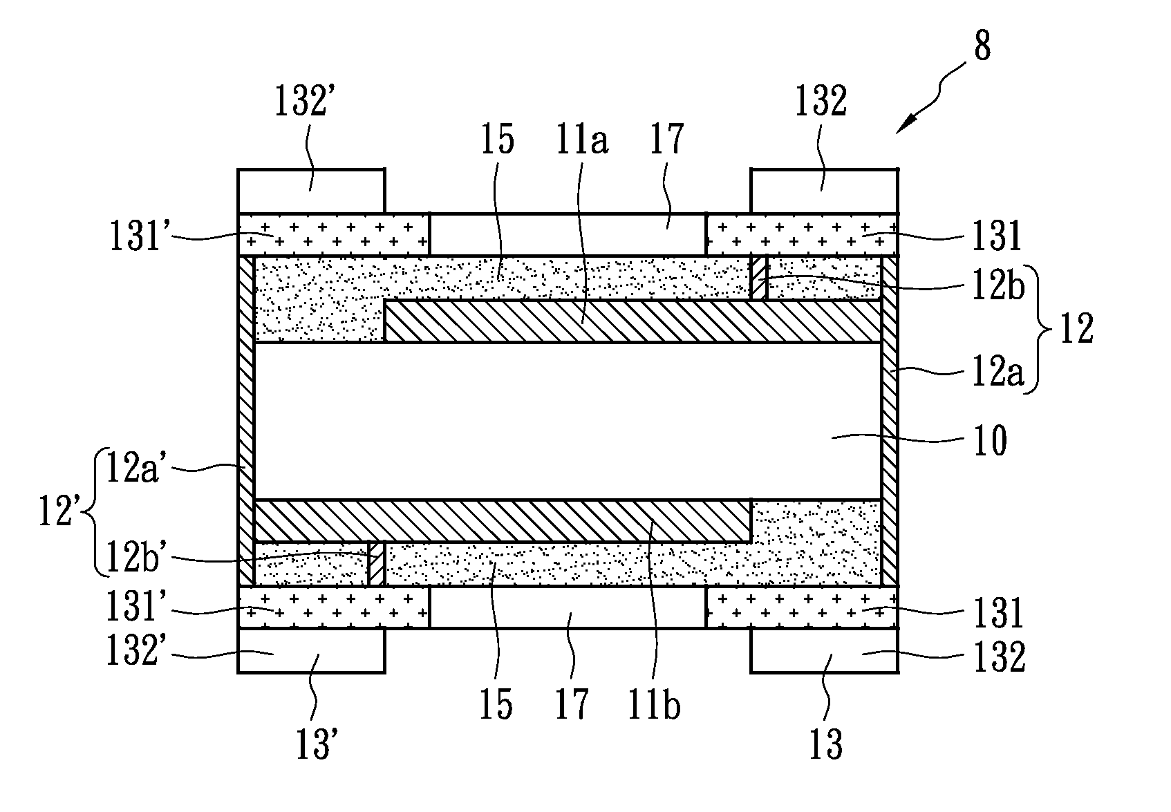
[0032]FIG. 4 illustrates the surface mountable over-current protection device 4. A first electrode 13 comprises a pair of first electrode layers 131, and a second electrode 13′ comprises a pair of second electrode layers 131′. A first connecting conductor 12 connects to the first electrode layers 131 and the first metal foils 11a, and the second connecting conductor 12′ connects to the second electrode layers 131′ and the second metal foils 11b. The first metal foil 11a is formed by etching and is electrically insulated from the second electrode 13′ and the second connecting conductor 12′ by an etching line 16 (or etching area). Similarly, the second metal foil 11b is formed by etching and is electrically insulated from the first electrode 13 and the first connecting conductor 12 by an etching line 16′ (or etching area). In this embodiment, A1 is the total area of the first electrode 13 and the second electrode 13′; A2 is the total area of the first connecting conductor 12 and the s...


PUM

PropertyMeasurementUnit
sizeaaaaaaaaaa
sizeaaaaaaaaaa
heat dissipation factoraaaaaaaaaa

Abstract

A surface-mountable over-current protection device comprises one PTC material layer, first and second connecting conductors, first and second electrodes and an insulating layer. The PTC material layer has a resistivity less than 0.2 Ω-cm, and comprises crystalline polymer and conductive filler dispersed therein. The first and second connecting conductors are capable of effectively dissipating heat generated from the PTC material layer. The first and second electrodes are electrically connected to first and second surfaces of the PTC material layer through the first and second connecting conductors, respectively. The dissipation factor depending on the ratio of the total area of the electrodes and the conductors to the area of the PTC material layer is greater than 0.6. At 25° C., the value of the hold current of the device divided by the product of the area of the PTC material layer and the number of the PTC material layer is greater than 1A / mm2.

Description

BACKGROUND OF THE INVENTION[0001](1) Field of the Invention[0002]The present application relates to a surface mountable over-current protection device, and more particularly to a surface mountable over-current protection device with high hold current and positive temperature coefficient (PTC) characteristics.[0003](2) Description of the Related Art[0004]Because the resistance of conductive composite materials having PTC characteristic is very sensitive to temperature variation, it can be used as the material for current sensing devices, and has been widely applied to over-current protection devices or circuit devices. The resistance of the PTC conductive composite material remains extremely low at normal temperature, so that the circuit or cell can operate normally. However, when an over-current or an over-temperature event occurs in the circuit or cell, the resistance instantaneously increases to a high resistance state (e.g., at least 102Ω), so as to suppress over-current and prot...

Claims


Application Information

Patent Timeline
Patent Type & Authority Patents(United States)
IPC IPC(8): H01C7/10H01C7/13H01C1/08H01C1/14H01C7/02H01C17/065
CPCH01C1/08H01C1/1406H01C7/027H01C7/021H01C17/0652H01C17/06526H01C17/06566
Inventor WANG, DAVID SHAU CHEWCHU, FU HUATSENG, CHUN TENG
Owner POLYTRONICS TECH
Why Eureka
Try Eureka