Edge-emitting etched-facet lasers

a technology of etched facets and laser chips, which is applied in the direction of semiconductor laser structure details, semiconductor lasers, individual semiconductor device testing, etc., can solve the problems of significantly reducing the number of useful laser chips that can be produced from a given wafer, and conventional lithographical techniques cannot be readily used to further process lasers. , to achieve the effect of minimising wasted spa

Active Publication Date: 2015-01-13
MACOM TECH SOLUTIONS HLDG INC
View PDF17 Cites 0 Cited by
  • Summary
  • Abstract
  • Description
  • Claims
  • Application Information

AI Technical Summary

Benefits of technology

[0005]In general, in one aspect, the invention features edge-emitting lasers that are able to be fabricated with minimal wasted space between adjacent lasers. The front etched facet of a laser is facing a recessed region on the back side of the adjacent laser chip so that the light from the front facet of a first laser can exit without interference and back-reflection from the back facet of a second adjacent laser.
[0006]The invention may include a chip with a first etched-facet edge-emitting semiconductor laser, the chip contains a recessed region to allow a second etched-facet edge-emitting semiconductor laser, adjacent to the chip containing the first laser and with its front-facet facing the chip, to be closely spaced to each other while avoiding distortion during the testing of the characteristics of the second laser. This allows a significant increase in the number of chips that can be produced from a wafer.
[0007]Other embodiments include one or more of the following features. The recessed region can have a slanted end wall to minimize back-reflection. The back facet of a laser may also face a recessed region on the front side of the adjacent laser chip and the recessed region may have an angled end wall. Chips may have a complete recessed region or complete opening along their length and offset from each other to minimize back reflection.
[0008]In one particular embodiment, a laser chip may comprise a substrate; an epitaxial structure on the substrate, the epitaxial structure including an active region, the active region generating light; a waveguide formed in the epitaxial structure extending in a first direction, the waveguide having a front etched facet and a back etched facet that define an edge-emitting laser; and a first recessed region formed in said epitaxial structure, the first recessed region being arranged at a distance from the waveguide and having an opening adjacent to the back etched facet, the first recessed region facilitating testing of an adjacent laser chip prior to singulation of the laser chip.
[0024]In another particular embodiment, a laser chip may comprise a substrate; an epitaxial structure on the substrate, the epitaxial structure including an active region, the active region generating light; a first waveguide formed in the epitaxial structure extending in a first direction, the first waveguide having a first front etched facet and a first back etched facet that define a first edge-emitting laser; a second waveguide formed in the epitaxial structure extending in the first direction, the second waveguide having a second front etched facet and a second back etched facet defining a second edge-emitting laser, a recessed region formed in said epitaxial structure, the recessed region having an opening adjacent to one of the first back etched facet and the second back etched facet, the recessed region facilitating testing of an adjacent laser chip prior to singulation of the laser chip.
[0027]In another particular embodiment, a laser chip may comprise a substrate; an epitaxial structure on the substrate, the epitaxial structure including an active region, the active region generating light; a waveguide formed in the epitaxial structure extending in a first direction, the waveguide having a front etched facet and a back etched facet that define an edge-emitting laser; and a complete opening in the epitaxial structure in a direction parallel to and at a distance from the waveguide facilitating testing of an adjacent laser chip prior to singulation of the laser chip.

Problems solved by technology

Since the semiconductor material is cleaved to form the laser facets, the locations and orientations of the facets are limited; furthermore, once the wafer has been cleaved it typically is in small pieces so that conventional lithographical techniques cannot readily be used to further process the lasers.
However, FP and DFB edge-emitting lasers fabricated using etched facets could not be closely packed because of the interference of the laser output from a front facet of laser to the back facet of the adjacent laser that would distort on-wafer test results.
For example, for a DFB laser, this wasted space is on the order of 100 μm that significantly reduces the number of useful laser chips that can be produced from a given wafer.

Method used


Image

  • Edge-emitting etched-facet lasers
  • Edge-emitting etched-facet lasers
  • Edge-emitting etched-facet lasers

Examples


Embodiment Construction

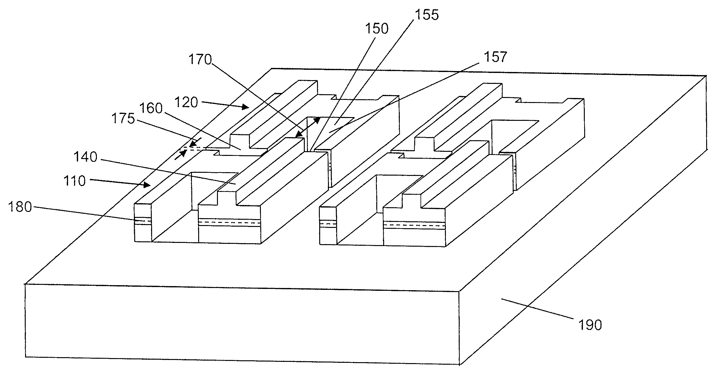
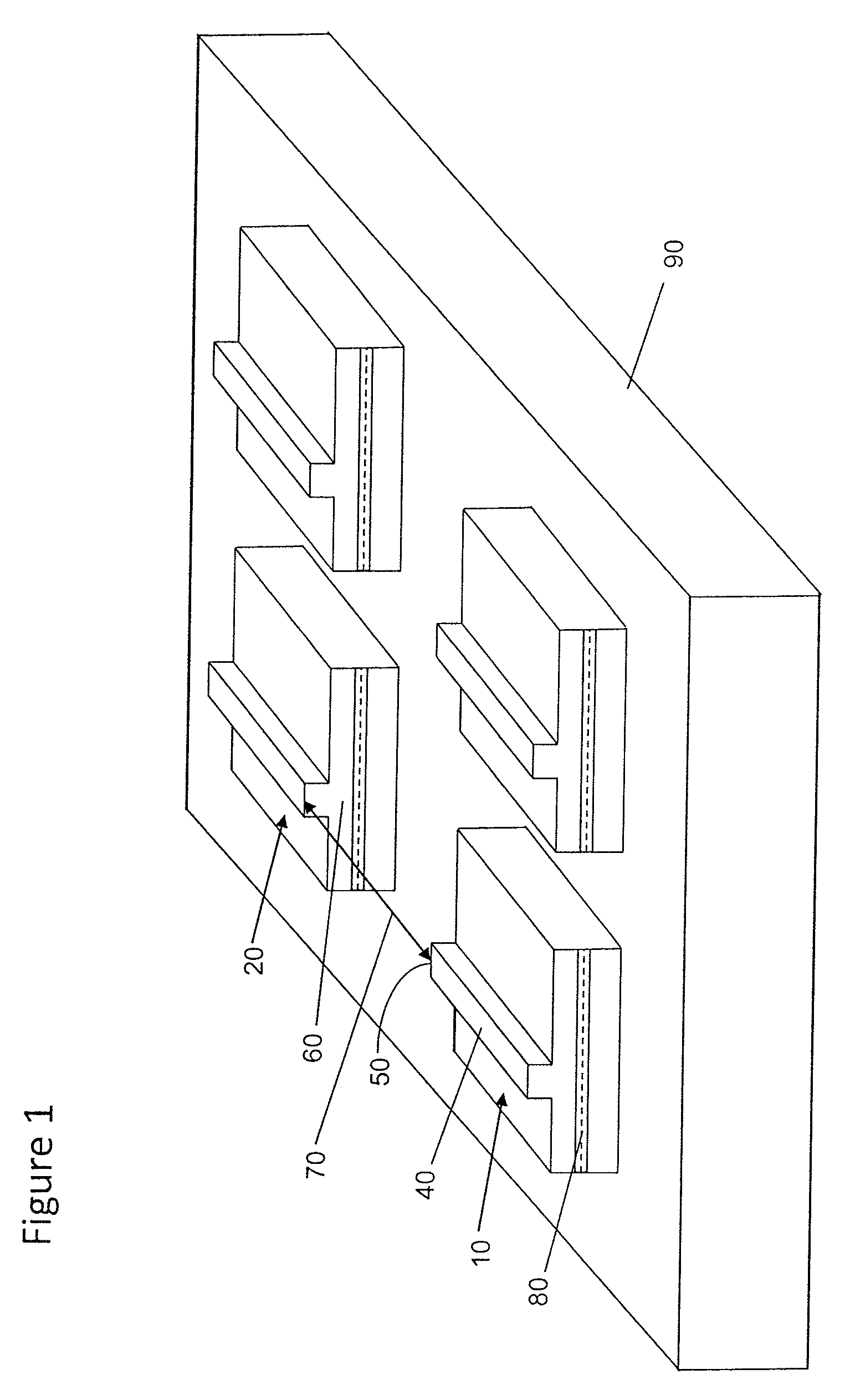
[0040]FIG. 1 shows a perspective view of a substrate 90 with an epitaxially deposited waveguide structure including an active region 80 in which etched-facet lasers including a ridge 40 are fabricated. The etched-facet ridge laser mesas 10 and 20 are positioned on the substrate so that the front facet 50 of laser corresponding to mesa 10 is at a distance 70 from the back facet of laser corresponding to mesa 20.

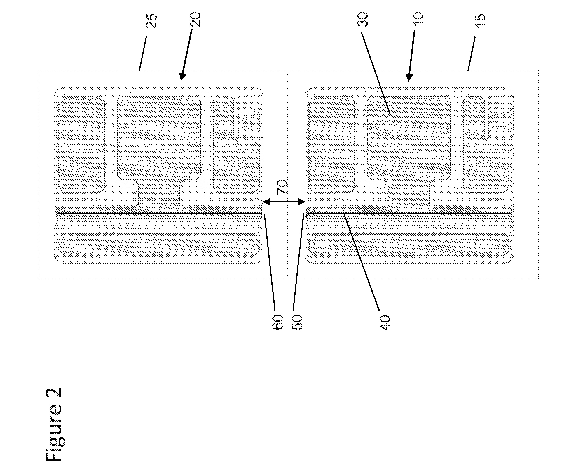
[0041]FIG. 2 shows a top plan view of two adjacent etched-facet ridge lasers, similar to those in FIG. 1. A wire-bond pad 30 is provided to allow wire-bonding to the pad and for electric current to be directed to the ridge allowing the laser to operate. The laser mesas 10 and 20 are positioned on chip 15 and 25, respectively. The chips 15 and 25 are formed through a singulation process along the lines that define the boundary of the chips in FIG. 2.

[0042]The substrate 90 may be formed, for example, of a type III-V compound, or an alloy thereof, which may be suitably doped. The...


PUM


Abstract

A laser chip having a substrate, an epitaxial structure on the substrate, the epitaxial structure including an active region and the active region generating light, a waveguide formed in the epitaxial structure extending in a first direction, the waveguide having a front etched facet and a back etched facet that define an edge-emitting laser, and a first recessed region formed in said epitaxial structure, the first recessed region being arranged at a distance from the waveguide and having an opening adjacent to the back etched facet, the first recessed region facilitating testing of an adjacent laser chip prior to singulation of the laser chip.

Description

CROSS-REFERENCE TO RELATED APPLICATIONS[0001]The present application claims the benefit of priority to U.S. Provisional Application No. 61 / 568,383, filed Dec. 8, 2011, and U.S. Provisional Application No. 61 / 619,190, filed Apr. 2, 2012, the entire contents of each of which is herein incorporated by reference.BACKGROUND OF THE INVENTION[0002]The present invention relates, in general, to etched-facet photonic devices, and more particularly to improved etched-facet photonic devices and methods for fabricating them.[0003]Semiconductor lasers typically are fabricated on a wafer by growing an appropriate layered semiconductor material on a substrate through Metalorganic Chemical Vapor Deposition (MOCVD) or Molecular Beam Epitaxy (MBE) to form an epitaxial structure having an active layer parallel to the substrate surface. The wafer is then processed with a variety of semiconductor processing tools to produce a laser optical cavity incorporating the active layer and incorporating metallic ...

Claims


Application Information

Patent Timeline
Patent Type & Authority Patents(United States)
IPC IPC(8): H01S5/026H01S5/00H01S5/02H01S5/028H01S5/12H01S5/20H01S5/22
CPCH01S5/20H01S5/0042H01S5/0203H01S5/22H01S5/0201H01S5/028G01R31/2635H01S5/12G01R31/26H01S5/0014H01S5/0287H01S5/1014H01S5/223H01S5/34306H01S5/34313H01S5/34333
Inventor BEHFAR, ALEX A.GREEN, MALCOLM R.STAGARESCU, CRISTIAN
Owner MACOM TECH SOLUTIONS HLDG INC
Why Eureka
Try Eureka