Supercharge Your Innovation With Domain-Expert AI Agents!

Packaged semiconductor device having multilevel leadframes configured as modules

a technology of semiconductor devices and modules, applied in semiconductor devices, semiconductor/solid-state device details, electrical devices, etc., can solve problems such as parasitic resistance and inductance, and achieve the effect of low cos

Active Publication Date: 2015-02-03
TEXAS INSTR INC
View PDF6 Cites 3 Cited by
  • Summary
  • Abstract
  • Description
  • Claims
  • Application Information

AI Technical Summary

Benefits of technology

This approach results in a compact, cost-effective power converter system that conserves board space, facilitates quick customization, and improves thermal management by allowing flexible component arrangement and reduced parasitic resistances.

Problems solved by technology

Even for close proximity between inductor and FETs, and to circuitry capacitors, there are connecting traces, which necessarily introduce parasitic resistances and inductances.

Method used


Image

  • Packaged semiconductor device having multilevel leadframes configured as modules
  • Packaged semiconductor device having multilevel leadframes configured as modules
  • Packaged semiconductor device having multilevel leadframes configured as modules

Examples


Embodiment Construction

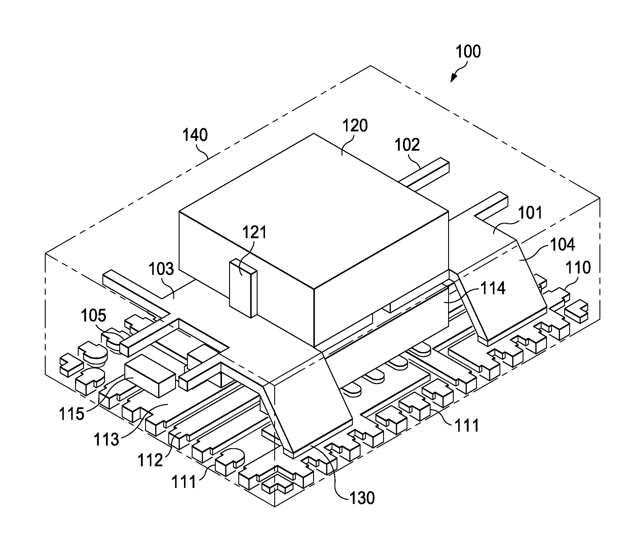
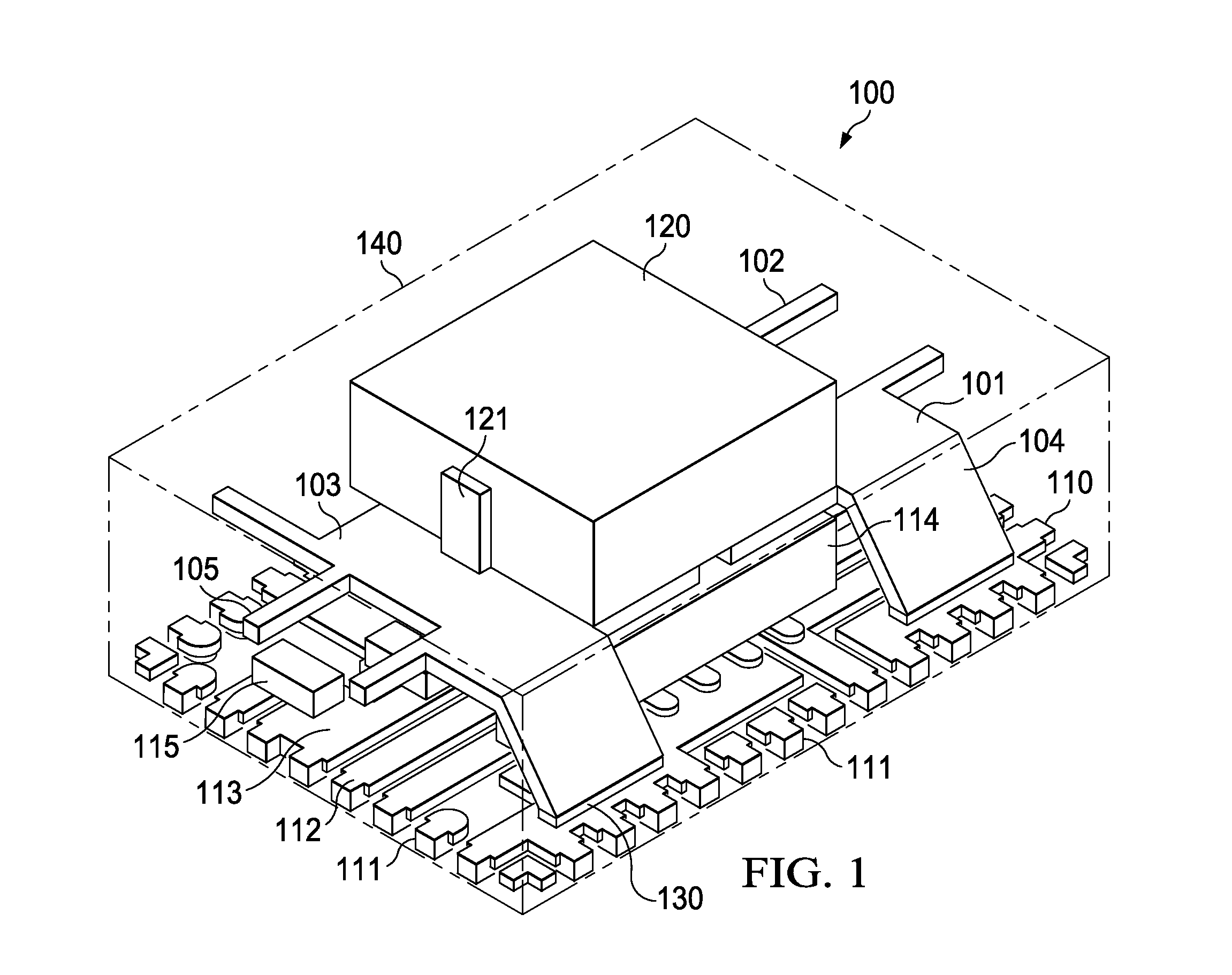
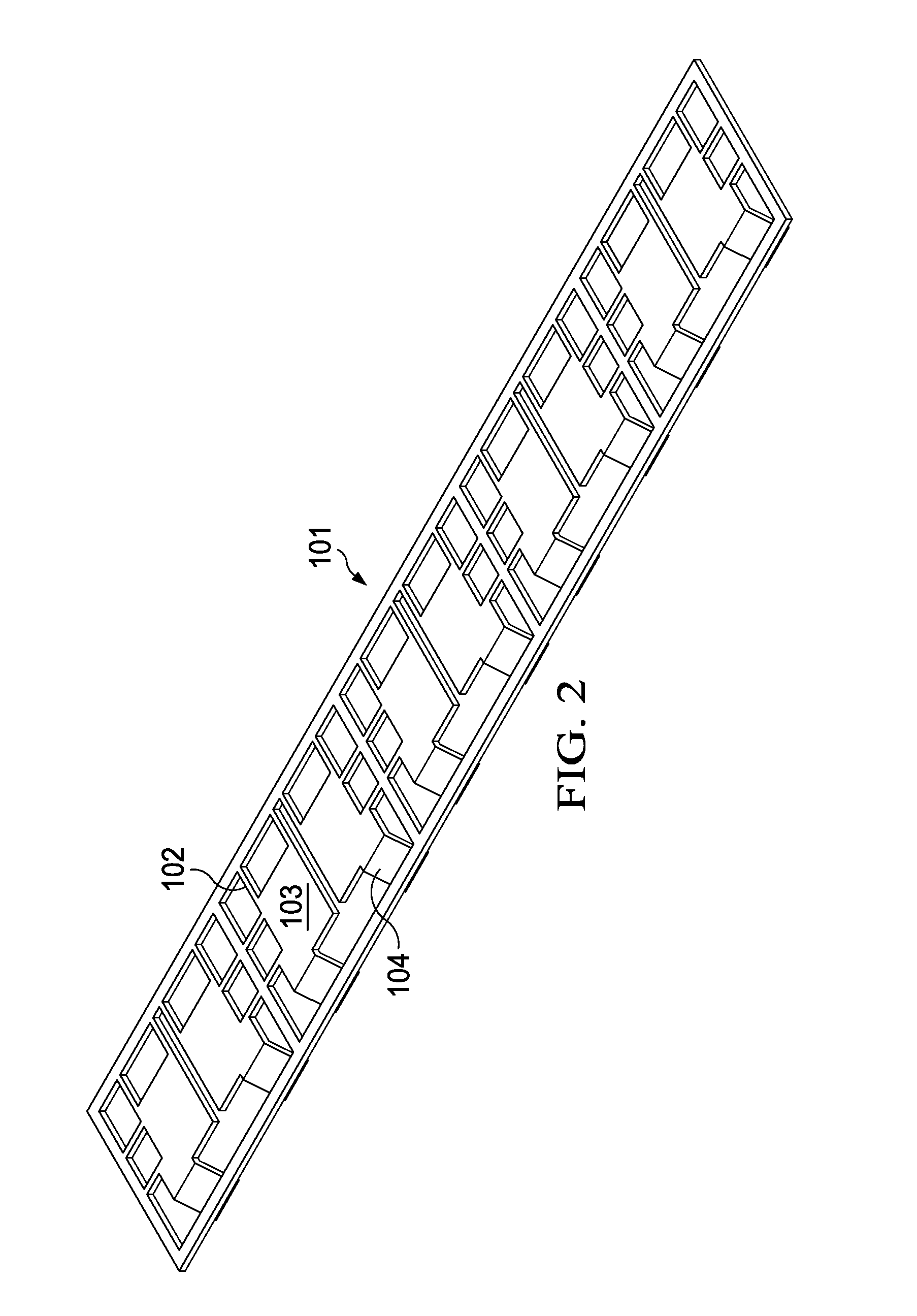
[0028]FIG. 1 displays a perspective view of an exemplary packaged electronic system generally designated 100. The system is based on two QFN / SON-type planar metal leadframes; the first planar leadframe is designated 101, the second planar leadframe is designated 110. Both leadframes include pads for attaching components, and leads for interconnection. Both leadframes are etched or stamped from sheets of metal, preferably in the thickness range from about 100 μm to 250 μm. Preferred metals include, but are not limited to, copper, copper alloys, iron-nickel alloys, aluminum, and Kovar™. The metal of the first leadframe is called the first metal, and the metal of the second leadframe is called the second metal. For some applications of the packaged system, it is a technical advantage that the metal of the second leadframe may be selected to be different from the first metal. Further, the metal thickness of the second leadframe may be the same as the metal thickness of the first leadfra...


PUM


Abstract

A semiconductor system (100) has a first planar leadframe (101) with first leads (102) and pads (103) having attached electronic components (120), the first leadframe including a set of elongated leads (104) bent at an angle away from the plane of the first leadframe; a second planar leadframe (110) with second leads (112) and pads (113) having attached electronic components (114); the bent leads of the first leadframe conductively connected to the second leadframe, forming a conductively linked 3-dimensional network between components and leads in two planes; and packaging material (140) encapsulating the 3-dimensional network.

Description

CROSS-REFERENCE TO RELATED APPLICATIONS[0001]This application claims the benefit of the filing date of U.S. Provisional Patent Application No. 61 / 615,002, which is titled “System in Package (SIPO with Stacked Inductor” and was filed on Mar. 23, 2012, the disclosure of which is hereby incorporated by reference herein in its entirety.FIELD OF THE INVENTION[0002]The present invention is related in general to the field of semiconductor devices and processes, and more specifically to structure and fabrication method of an electronic system having interconnected modular multilevel leadframes.DESCRIPTION OF RELATED ART[0003]Among the long-term trends in semiconductor technology which continue unabated are the trends towards miniaturization, integration, and speed. In addition to these trends, recent years have shown emerging product demands for greater flexibility to satisfy customization of products and for reducing the time needed to bring these products to market. A specific product exa...

Claims


Application Information

Patent Timeline
Patent Type & Authority Patents(United States)
IPC IPC(8): H01L23/02H01L21/56H01L23/00H01L23/31H01L23/495
CPCH01L23/49568H01L23/49575H01L21/56H01L24/97H01L23/495H01L23/49537H01L23/49551H01L21/561H01L23/3107H01L2924/15747H01L2924/181H01L2224/40245H01L24/38H01L21/52H01L25/50H01L2224/8485H01L2224/84801H01L24/84H01L24/40H01L24/37H01L2224/37013H01L2924/00H01L2924/0781H01L2924/00014H01L2924/00012
Inventor SAYE, RICHARD J.
Owner TEXAS INSTR INC
Features
  • R&D
  • Intellectual Property
  • Life Sciences
  • Materials
  • Tech Scout
  • Unparalleled Data Quality
  • Higher Quality Content
  • 60% Fewer Hallucinations
Learn More