Electromagnetic interference noise reduction package board

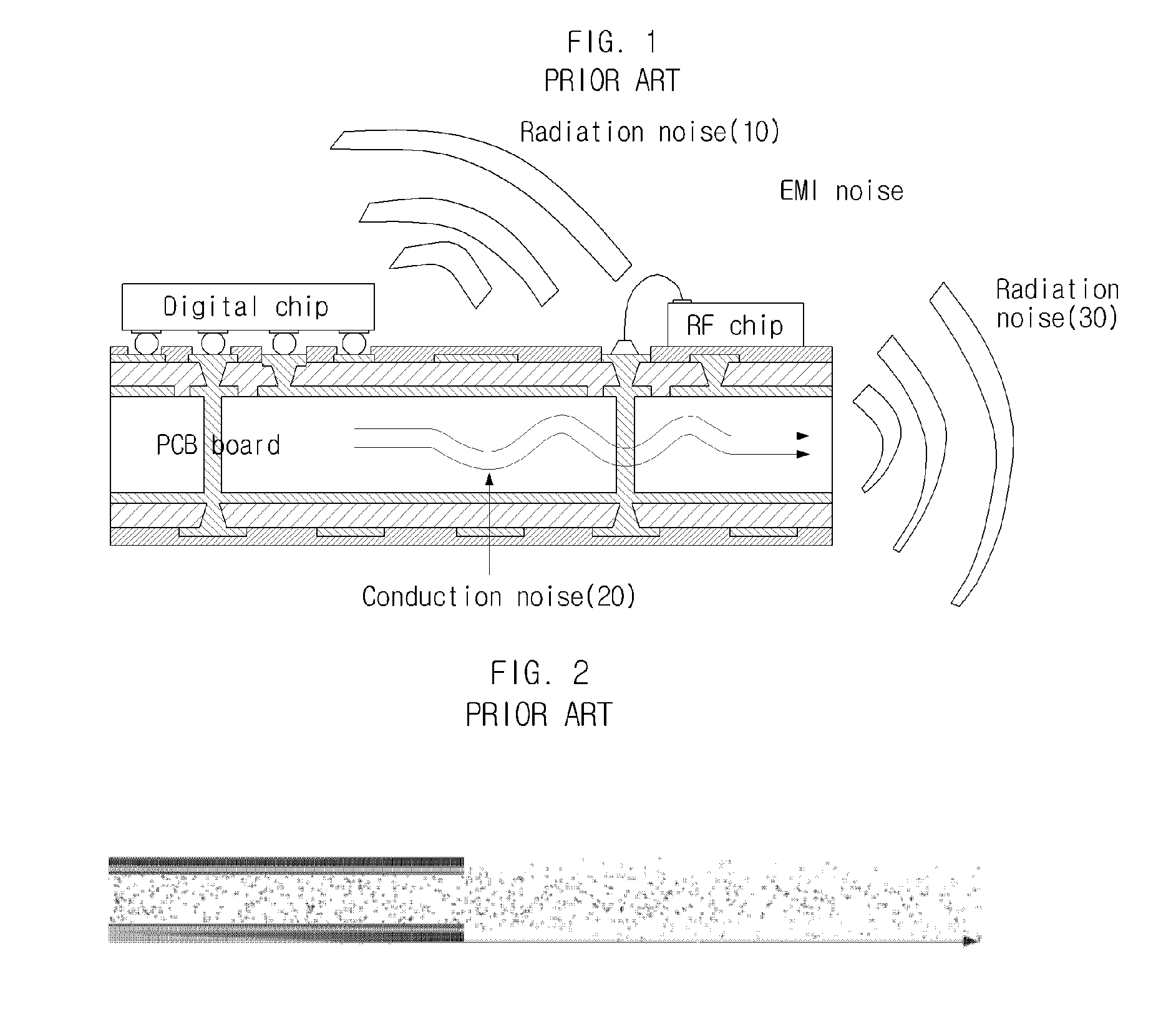
a technology of noise reduction and electronic interference, applied in the field of boards, can solve the problems of limiting the ability to shield the noise completely on the board, emi has become a chronic noise problem, and emi has become increasingly serious

Inactive Publication Date: 2015-02-10
SAMSUNG ELECTRO MECHANICS CO LTD
View PDF4 Cites 2 Cited by
  • Summary
  • Abstract
  • Description
  • Claims
  • Application Information

AI Technical Summary

Benefits of technology

[0010]The present invention provides an EMI noise reduction package board that can shield radiation noise radiated at an edge of the board, by inserting an electromagnetic bandgap structure that can shield the noise in a particular frequency band into the edge of the board.
[0011]The present invention provides an EMI noise reduction package board that has advantages in terms of spatial utilization, manufacturing cost and power consumption because radiation noise radiated at an edge of the board can be easily shielded by a simple structural change of the board.

Problems solved by technology

As the operating frequencies of electronic products become higher, electromagnetic interference (EMI) has become a chronic noise problem.
Particularly, as the recent electronic products are operated in a double-digit MHz to a few GHz, the EMI problem has become increasingly serious, making it urgent to find a solution.
Among the EMI problems in a board, there have been few studies targeted for the noise occurred at an edge of the board, limiting the ability to shield the noise completely on the board.
An EMI noise refers to a noise that causes a noise problem generated by interference when electromagnetic waves generated in one electronic circuit, device or part is transferred to another electronic circuit, device or part.
However, there have been insufficient studies for an effective solution for the radiation noise 30 (simply referred to as “edge noise”), which is the conduction noise 20 flowing through the inside of the board that is conducted to an edge of the board and radiated to the outside of the board.

Method used


Image

  • Electromagnetic interference noise reduction package board
  • Electromagnetic interference noise reduction package board
  • Electromagnetic interference noise reduction package board

Examples


Embodiment Construction

[0023]Since there can be a variety of permutations and embodiments of the present invention, certain embodiments will be illustrated and described with reference to the accompanying drawings. This, however, is by no means to restrict the present invention to certain embodiments, and shall be construed as including all permutations, equivalents and substitutes covered by the ideas and scope of the present invention.

[0024]Throughout the description of the present invention, when describing a certain technology is determined to evade the point of the present invention, the pertinent detailed description will be omitted. Numerals (e.g., first, second, etc.) used in the description of the present invention are only for distinguishing one element from another element.

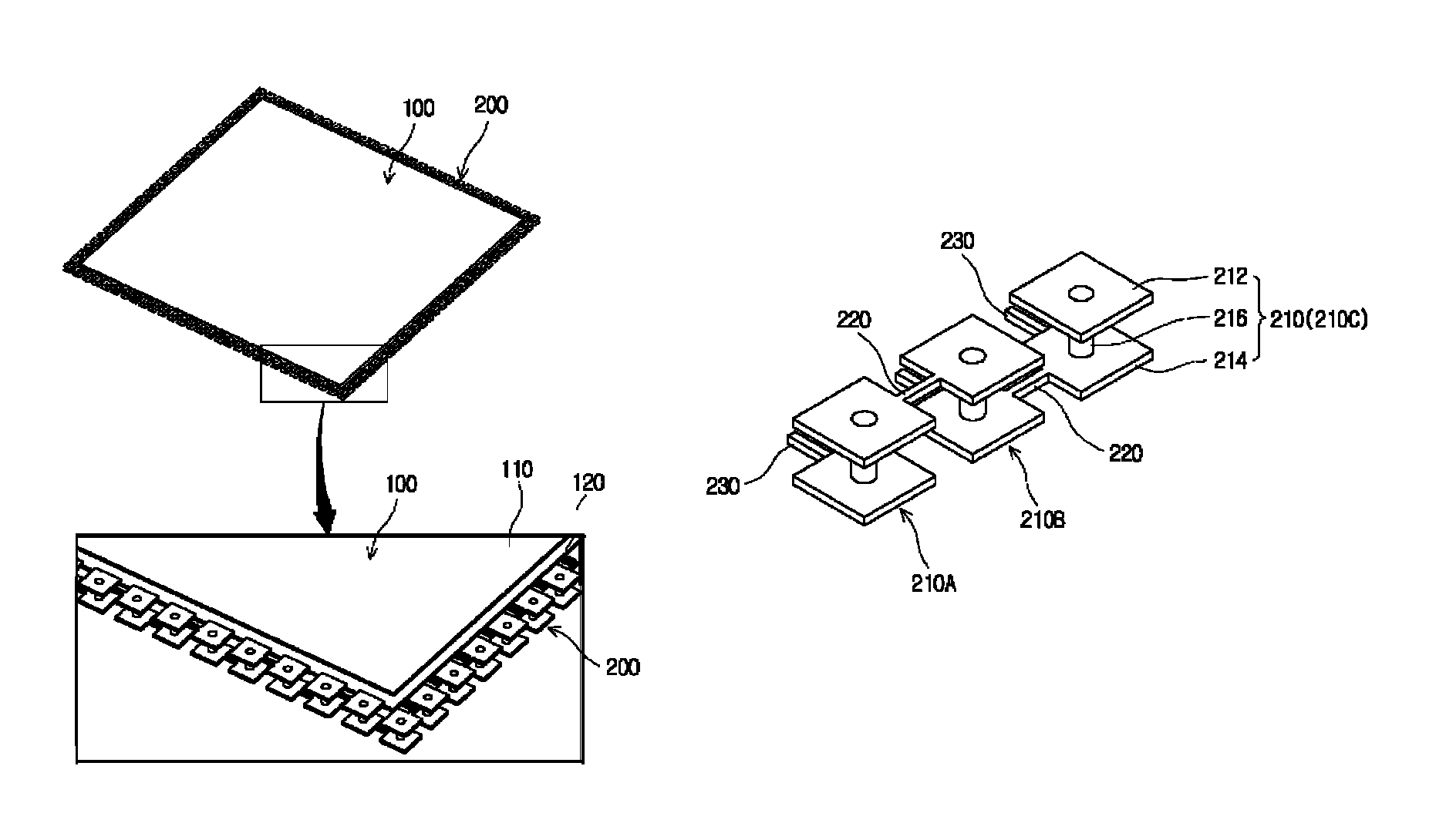
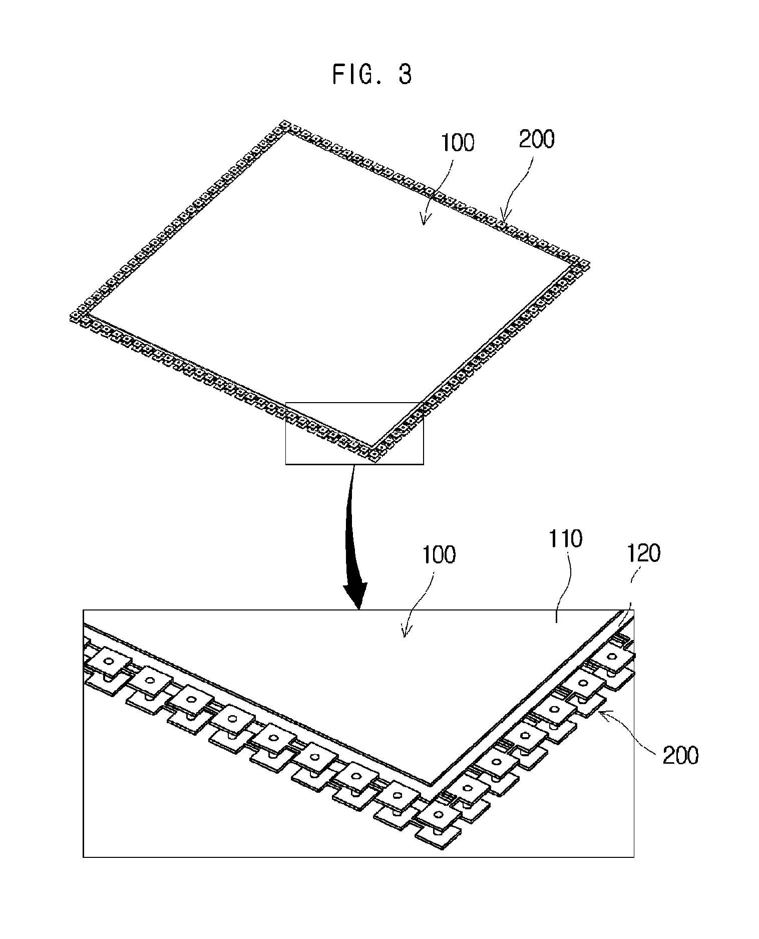
[0025]Hereinafter, an EMI noise reduction package board in accordance with an embodiment of the present invention will be described in detail with reference to the accompanying drawings. Identical or corresponding elements wi...


PUM


Abstract

An EMI noise reduction package board, having a top layer and a bottom layer, one of which having a semiconductor device mounted thereon, can include: a first area having a signal layer arranged on one surface thereof; and a second area placed on a lateral side of the first area and having unit structures arranged repeatedly therein, the unit structures configured for inhibiting EMI noise from being radiated to an outside through the lateral side of the first area. The unit structure can include: a top conductive plate and a bottom conductive plate, formed, respectively, on the top layer and the bottom layer of the second area to face each other in a pair; and a via, connecting the top conductive plate with the bottom conductive plate.

Description

CROSS-REFERENCE TO RELATED APPLICATIONS[0001]This application claims the benefit of Korean Patent Application No. 10-2011-0083674, filed with the Korean Intellectual Property Office on Aug. 22, 2011, the disclosure of which is incorporated herein by reference in its entirety.BACKGROUND[0002]1. Technical Field[0003]The present invention relates to a board, more specifically to a noise reduction board that can reduce electromagnetic interference noise by use of an electromagnetic bandgap structure.[0004]2. Background Art[0005]As the operating frequencies of electronic products become higher, electromagnetic interference (EMI) has become a chronic noise problem. Particularly, as the recent electronic products are operated in a double-digit MHz to a few GHz, the EMI problem has become increasingly serious, making it urgent to find a solution. Among the EMI problems in a board, there have been few studies targeted for the noise occurred at an edge of the board, limiting the ability to sh...

Claims


Application Information

Patent Timeline
Patent Type & Authority Patents(United States)
IPC IPC(8): H05K1/11H01L23/552H01L23/64H01L23/66H05K1/02
CPCH01L23/64H01L23/552H05K1/0236H05K1/0224H01L23/66H01L2224/16225H01L2224/48091H01L2224/48227H01L2924/00014
Inventor KIM, HANPARK, DAE-HYUNBAN, YOUNG-MIN
Owner SAMSUNG ELECTRO MECHANICS CO LTD
Why Eureka
Try Eureka