Nonvolatile semiconductor memory device and read method for the same

a nonvolatile semiconductor and memory device technology, applied in information storage, static storage, digital storage, etc., can solve the problems of increasing the demand for large capacity of nonvolatile memory devices, increasing the cost of products, so as to reduce detection sensitivity and improve reading accuracy

Active Publication Date: 2015-02-10
PANASONIC SEMICON SOLUTIONS CO LTD
View PDF16 Cites 27 Cited by
  • Summary
  • Abstract
  • Description
  • Claims
  • Application Information

AI Technical Summary

Benefits of technology

[0023]In a cross point nonvolatile semiconductor memory device which uses a variable resistance memory element of the present invention, the problem related to a cross-point circuit, i.e., the problem of reduced detection sensitivity due to sneak current at the time of reading a resistance value of a memory element can be prevented, and thus the effect of improved reading accuracy is achieved.

Problems solved by technology

Therefore, demand for large capacity of a nonvolatile memory device, low write power, high speed writing / reading, and long product life is increasing.
The sneak current prevents accurate detection of the resistance value of a memory element included in a read-target memory cell.
However, the sneak current increases according to the scale of a cross-point cell array, thereby preventing production of large scale cross-point cell arrays.

Method used


Image

  • Nonvolatile semiconductor memory device and read method for the same
  • Nonvolatile semiconductor memory device and read method for the same
  • Nonvolatile semiconductor memory device and read method for the same

Examples


embodiment

[Embodiment]

[0060]Hereinafter, an embodiment of the present invention will be described with reference to the drawings. Each of the embodiments described below illustrates a specific example of the present invention. Numerical values, shapes, materials, components, arrangement positions and topologies of the components, steps, and order of the steps shown in the following embodiments are examples, and not intended to limit the present invention. Those components in the following embodiments, which are not stated in the independent claim that defines the most generic concept are each described as an arbitrary component.

[0061]The same element may be labeled with the same symbol and description thereof may be omitted.

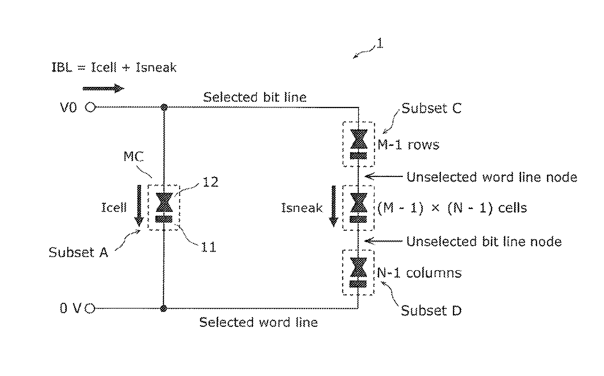
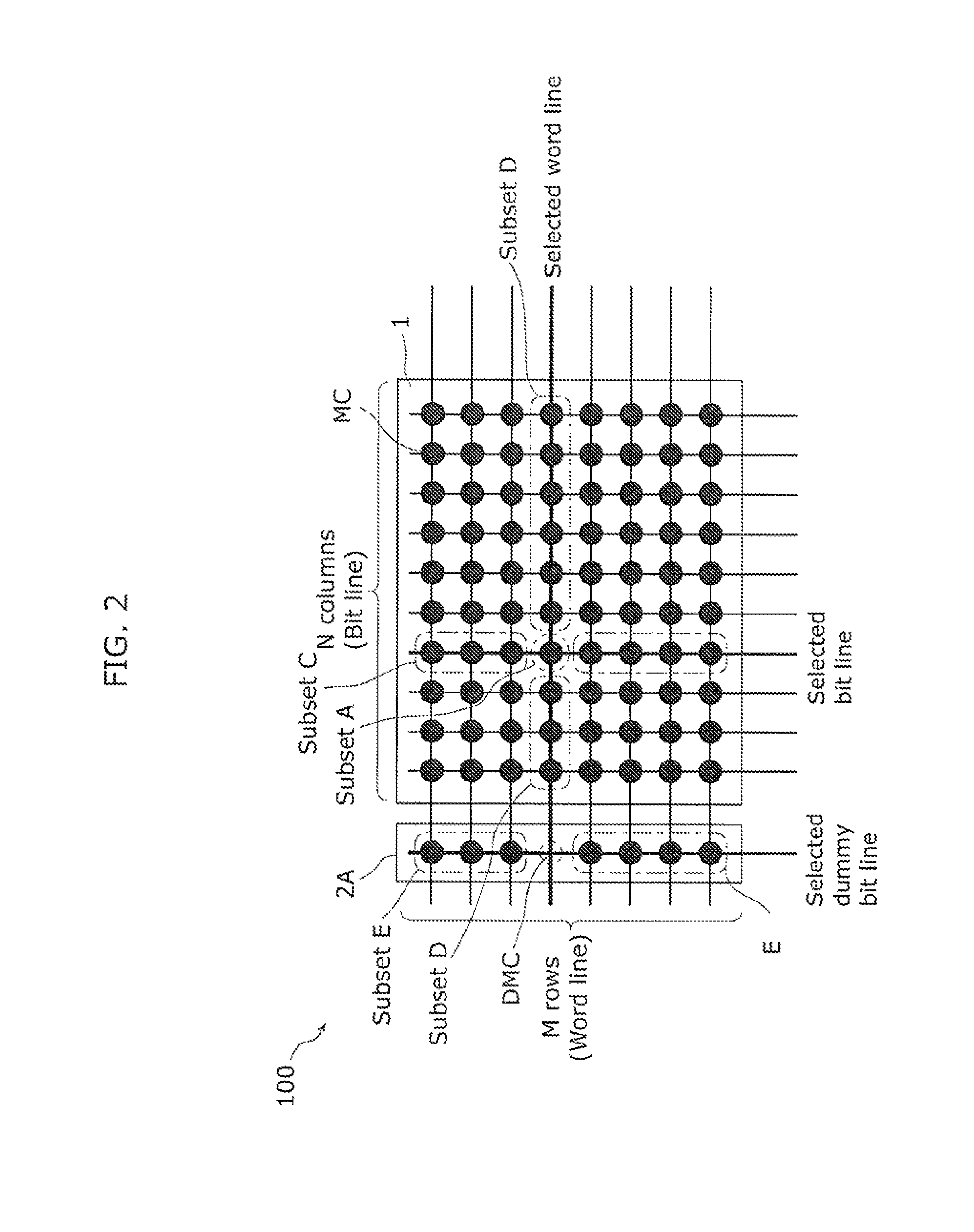
[0062]In the present invention, the configurations of memory elements and wiring are schematically illustrated. In addition, the numbers of memory elements and wiring are adjusted for the purpose of clarity of illustration.

[0063]Although only cross-point cell array with on...

first embodiment

[First Embodiment]

[0130]FIG. 8 is a block diagram illustrating the circuit configuration of a nonvolatile semiconductor memory device 200 in a first embodiment of the present invention.

[0131]The nonvolatile semiconductor memory device 200 includes the following configuration as the main components. The nonvolatile semiconductor memory device 200 includes word lines WL0 to WL7 formed in parallel in a first plane; bit lines formed in parallel in a second plane and three-dimensionally crossing the word lines WL0 to WL7, the second plane being parallel to the first plane; and a first cross-point cell array (cross-point cell array 1) including first type cells (memory cells) located at three-dimensional cross-points of the word lines WL0 to WL7 and the bit lines. The nonvolatile semiconductor memory device 200 further includes one or more dummy bit lines (here, four dummy bit lines DBL0 to DBL3) formed in parallel and three-dimensionally crossing the word lines WL0 to WL7 in the second p...

second embodiment

[Second Embodiment]

[0158]FIG. 11 is a block diagram illustrating the circuit configuration of a nonvolatile semiconductor memory device 300 in a second embodiment of the present invention. The nonvolatile semiconductor memory device 300 generates a determination level of the sense amplifier with high accuracy by utilizing the result that the current which flows through the dummy bit line corresponds to the sneak current in Expression 2.

[0159]The nonvolatile semiconductor memory device 300 includes the following configuration as the main components. That is to say, similarly to the nonvolatile semiconductor memory device 200 of FIG. 8, the nonvolatile semiconductor memory device 300 includes word lines WL0 to WL7 formed in parallel in a first plane; bit lines formed in parallel in a second plane and three-dimensionally crossing the word lines WL0 to WL7, the second plane being parallel to the first plane; a first cross-point cell array (cross-point cell array 1) including first type ...


PUM


Abstract

A cross point nonvolatile memory device capable of suppressing sneak-current-caused reduction in sensitivity of detection of a resistance value of a memory element is provided. The device includes perpendicular bit and word lines; a cross-point cell array including memory cells each having a resistance value reversibly changing between at least two resistance states according to electrical signals, arranged on cross-points of the word and bit lines; an offset detection cell array including an offset detection cell having a resistance higher than that of the memory cell in a high resistance state, the word lines being shared by the offset detection cell array; a read circuit (a sense amplifier) that determines a resistance state of a selected memory cell based on a current through the selected bit line; and a current source which supplies current to the offset detection cell array in a read operation period.

Description

TECHNICAL FIELD[0001]The present invention relates to a cross point nonvolatile semiconductor memory device which uses a variable resistance memory element, and particularly, to a cell array structure which improves determination performance for a read command signal, and to a read method for the read command signal.BACKGROUND ART[0002]In recent years, along with the development of digital technology, functions of electronic devices such as portable information devices and information home appliances have been further improved. Therefore, demand for large capacity of a nonvolatile memory device, low write power, high speed writing / reading, and long product life is increasing.[0003]In order to meet such a demand, more finely structured flash memory using an existing floating gate is being developed.[0004]On the other hand, research and development of a nonvolatile memory device having a memory element including a so-called variable resistance memory element as a replacement for a fla...

Claims


Application Information

Patent Timeline
Patent Type & Authority Patents(United States)
IPC IPC(8): G11C11/00G11C7/14G11C11/16G11C13/00
CPCG11C13/004G11C11/1673G11C7/14G11C2213/71G11C2213/72G11C2213/73G11C2213/77G11C13/0004G11C2013/0054
Inventor SHIMAKAWA, KAZUHIKOTSUJI, KIYOTAKAAZUMA, RYOTARO
Owner PANASONIC SEMICON SOLUTIONS CO LTD
Why Eureka
Try Eureka