Check patentability & draft patents in minutes with Patsnap Eureka AI!

Method and architecture for improving defect detectability, coupling area, and flexibility of NVSRAM cells and arrays

a defect detection and array technology, applied in the field of methods and architectures, can solve the problems of unsuitable high-density nand and other flash cells, lack of flexibility in association, unreliable “store” operation, etc., and achieve the effect of increasing the coupling area and fast screening out defective bits

Inactive Publication Date: 2015-02-24
APLUS FLASH TECH
View PDF34 Cites 2 Cited by
  • Summary
  • Abstract
  • Description
  • Claims
  • Application Information

AI Technical Summary

Benefits of technology

The present invention provides improved techniques and methods for operating non-volatile static random-access memory (NVSRAM) cells and arrays. More particularly, the invention provides a flash cell margininal-Vt detector for screening out defective bits, a method for increasing coupling area for self-boosting program-inhibit cell operation, and a NVSRAM cell structure with at least two flash paired cells associated with each SRAM cell for cell recall / store flexibility. Other embodiments include increasing flash cell's coupling ratio and channel length for better performance and reliability, as well as a method for increasing the spacing between flash cells to prevent electron injection. Additionally, the invention provides an on-chip NVSRAM cell bit that can toggle "recall and store" operations between two flash bits for secure program-inhibit without degrading program performance.

Problems solved by technology

But practically, this is not suitable for today's high-density NAND and other flash cells because there is no Poly1-wing extending over the field region in extremely high-density Flash design wherein the Poly1 layer is usually made self-aligned to active layer for cell size reduction.
In yet another aspect of the NVSRAM cells and arrays, one drawback is lack of flexibility in association with a basic “store” operation followed by a “recall” operation to properly handle required erase operation on Flash part of the NVSRAM cell.
All these operations take time and have to be operated under the dropping VDD voltage, thus it makes the “store” operation very risky and unreliable.

Method used


Image

  • Method and architecture for improving defect detectability, coupling area, and flexibility of NVSRAM cells and arrays
  • Method and architecture for improving defect detectability, coupling area, and flexibility of NVSRAM cells and arrays
  • Method and architecture for improving defect detectability, coupling area, and flexibility of NVSRAM cells and arrays

Examples


case1

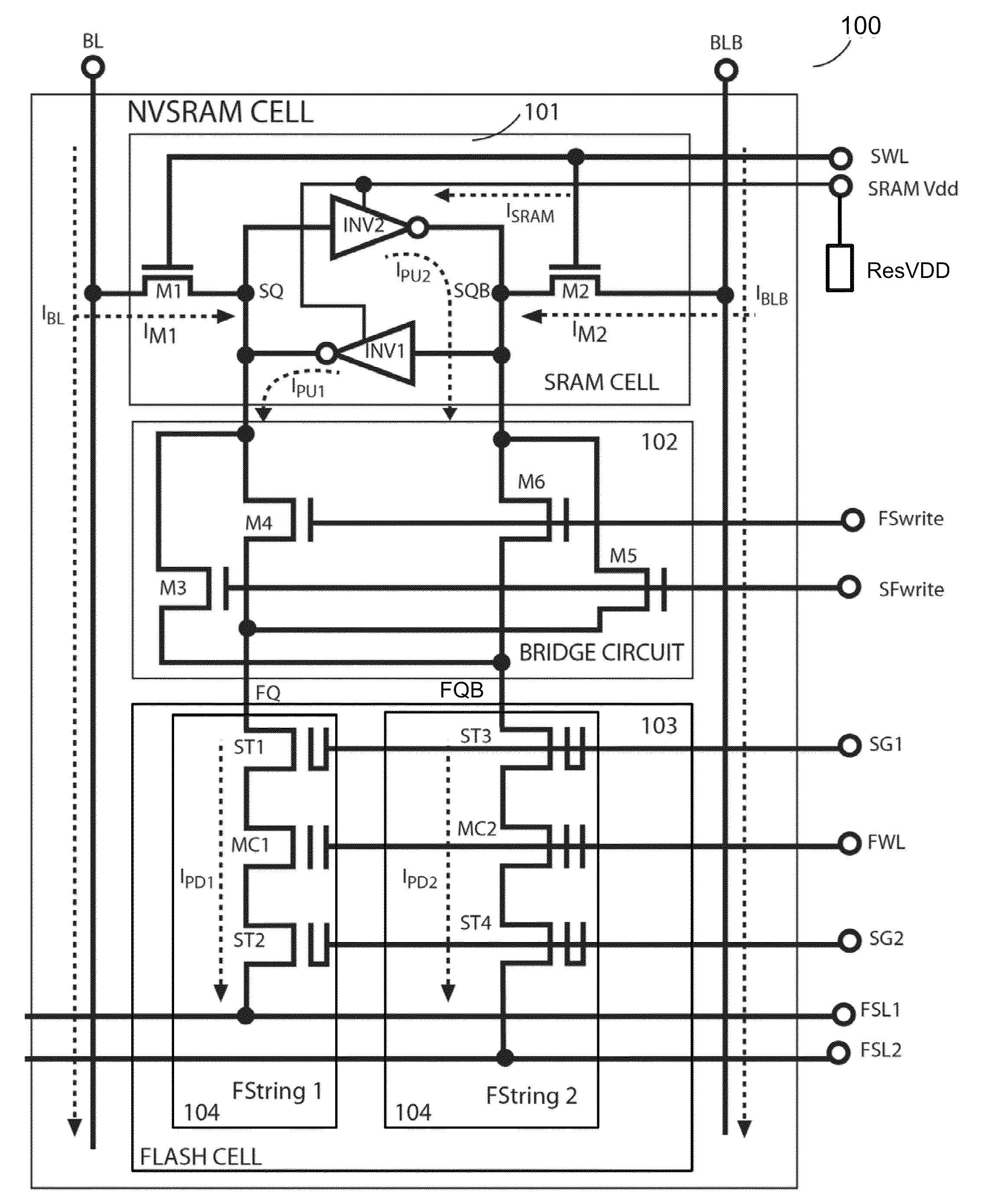
[0118]Now, the detailed operations of FSwrite and SFwrite of the preferred 1S1F 2-poly NMOS 16T NVSRAM cell shown in FIG. 1A will be explained below.[0119]1) FSwrite operation:[0120]Case1: FSwrite for writing Flash Logic “0” state into SRAM.[0121]The operation of Case1 is illustrated with reference to DA1 explained above. There are two ways to write each Flash stored logic state into each SRAM. One way is to write each Flash cell logic data into each corresponding SRAM cell with the same polarity in Logic state by setting FSwrite=VDD and SFwrite=VSS. The other way is to write each Flash cell logic data into each corresponding SRAM cell with opposite polarity in Logic state by setting FSwrite=VSS and SFwrite=VDD. The FSwrite operation is under LV (low voltage VDD) operation. All related control signals of SG1, FWL, FSL1, FSL2 and SWL are all coupled to LV VDD.[0122]In application, FSwrite operation is performed upon a power-on period. For a LV operation like 1.2V VDD, this operation ...


PUM


Abstract

Several preferred embodiments of 1S1F 16T NVSRAM, 1S1F 20T NVSRAM, 1S2F 22T NVSRAM, 1S2F 14T NVSRAM cells are proposed, regardless of 1-poly, 2-poly, PMOS or NOS flash cell structures. Two separate sourcelines for the paired flash Strings are also proposed for easy adding ability for the NVSRAM circuit to detect the marginally erased Vt0 and marginally programmed Vt1 of the paired flash cell. By increasing an resistance added to common SRAM power line, the pull-down current through flash Strings to grounding source line can be made much larger than the pull-up current to improve SFwrite program operation. Simple method by increasing flash cell channel length to effectively enhance coupling area is applied to secure SRAM-to-Flash store operation under self-boost-program-inhibit scheme. 1S2F architecture also provide flexibility for alternate erasing and programming during both a recall and store operation.

Description

CROSS-REFERENCES TO RELATED APPLICATIONS[0001]This application claims priority to U.S. Provisional Patent Application No. 61 / 705,597, filed on Sep. 25, 2012 and U.S. Provisional Patent Application No. 61 / 710,573, filed on Oct. 5, 2012, commonly assigned, and hereby incorporated by reference in its entirety herein for all purposes.[0002]Additionally, this application is related to U.S. Pat. Nos. 8,120,966, 8,120,959, 8,072,811, 7,688,612, 7,830,713, 8,233,320, 8,149,622, and U.S. patent applications Ser. No. 13 / 135,220, 13 / 199,785, 13 / 199,527, 13 / 888,134, 12 / 807,997, 61 / 275,148, 61 / 277,208, 61 / 574,632, and 61 / 687,227, commonly assigned, which are incorporated by reference herein for all purposes.[0003]Furthermore, this application is related to U.S. Pat. Nos. 5,065,362, 7,164,608, and 7,760,540.TECHNICAL FIELD OF THE INVENTION[0004]The present invention relates to several improved techniques and methods for operating the next-generation low-power Non-Volatile Static Random-Access Mem...

Claims


Application Information

Patent Timeline
Patent Type & Authority Patents(United States)
IPC IPC(8): G11C16/04G11C11/00G11C14/00H01L21/02
CPCG11C14/0063G11C11/005H01L21/0262G11C15/046G11C16/0483H01L27/0207H10B10/12H10B69/00
Inventor LEE, PETER WUNG
Owner APLUS FLASH TECH
Features
  • R&D
  • Intellectual Property
  • Life Sciences
  • Materials
  • Tech Scout
  • Unparalleled Data Quality
  • Higher Quality Content
  • 60% Fewer Hallucinations
Learn More