Clock-embedded source synchronous semiconductor transmitting and receiving apparatus and semiconductor system including same

a clock-embedded source and synchronous technology, applied in the field of semiconductor systems and semiconductor transmission/reception apparatuses, can solve problems such as jitter noise, change of data signal transition time, and increase of bit error rate (ber) attributable to power line noise inside and outside the chips

Inactive Publication Date: 2015-03-10
LEE KYONGSU
View PDF11 Cites 1 Cited by
  • Summary
  • Abstract
  • Description
  • Claims
  • Application Information

AI Technical Summary

Benefits of technology

[0008]The present invention has been made to resolve the problems of the existing transmission / reception method between semiconductor chips, and an object of the present invention is to provide a semiconductor transmission / reception apparatus using embedded source synchronous signaling, wherein a clock signal is combined with a differential data signal and transmitted, and a reception unit separates the clock signal and the differential data signal with ease and uses the signals for data recovery, thereby being capable of decreasing BER by minimizing a path difference occurring between the transmission and reception of data and a clock signal, that is, a problem in the existing clock-forwarded signaling method, and being capable of increasing power efficiency and reducing a load of the area of a transmission / reception circuit by removing a load of a complicated CDR circuit compared to the clock-embedded signaling method, and a semiconductor system including the same.

Problems solved by technology

As data transmission / reception rate between semiconductor chips increases, an increase of a Bit Error Rate (BER) attributable to noise on the power lines that is present inside and outside the chips becomes an important issue.
Such noise results in jitter noise by which the transition time of a data signal is changed.
As a result, the jitter noise functions as an important factor that limits maximum data transfer rate.
If such jitter noise differently affects the data signal and the clock signal on the path along which data synchronized with the clock signal at the transmitter is transferred to the reception unit through a communication channel, a cross correlation between the data and the recovery clock signal at the end of the channel is deteriorated when the reception unit recovers the data from the clock signal, leading to an increase of the BER.
In the former case, there often exists a difference between the transmission / reception paths of the data signal and the clock signal, and a difference of time delay on the paths attributable to parasitic capacitance and resistance components associated with a difference in the routing topology of the lines of the signals.
Such a phenomenon results in a great path difference especially when recovering the data from multiple transmission / reception channels using a single clock signal.
Furthermore, a difference in the routing topology of a medium conductor (or a transmission channel) that connects semiconductor chips on the outside of the semiconductor chips, that is, on a PCB makes this method as a disadvantageous method in high-speed signal transmission / reception because it often causes a difference in the path between data and the clock signal.
In this case, however, a CDR circuit itself is complicated, and the fast varying jitter noise of a data signal that is affected by rapidly changing power noise is not sufficiently rapidly incorporated into the clock signal due to the time delay of the CDR circuit itself.
Furthermore, such a method is disadvantageous in that it deteriorates power efficiency because the CDR circuit needs to operate continuously while data is transmitted.

Method used


Image

  • Clock-embedded source synchronous semiconductor transmitting and receiving apparatus and semiconductor system including same
  • Clock-embedded source synchronous semiconductor transmitting and receiving apparatus and semiconductor system including same
  • Clock-embedded source synchronous semiconductor transmitting and receiving apparatus and semiconductor system including same

Examples


Embodiment Construction

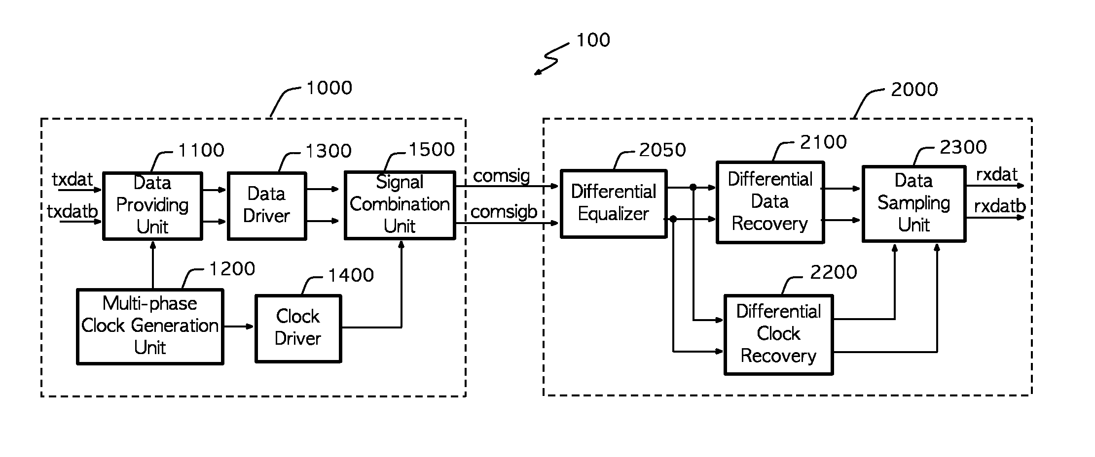
[0075]FIG. 9 is a block diagram illustrating an example of a semiconductor device in accordance with another embodiment of the present invention. FIG. 9 illustrates one implementation example of the first semiconductor device 1000 for sending differential data.

[0076]As illustrated in FIG. 9, the first semiconductor device 1000 may include a multiplexer 1100, that is, a data providing unit, a clock source 1200, that is, a clock generation unit, a data driver 1300, a clock driver 1400, and a phase shifter 1700. The multiplexer 1100, the data driver 1300 and the clock driver 1400 have the same construction as those of FIG. 1 and operate like those of FIG. 1, and a detailed description thereof is omitted.

[0077]The clock source 1200 may generate only a single clock signal, or may generate two single-clock signals having opposite phases. For example, two single clock signals having phases of 0 degree and 180 degrees are generated and provided to the multiplexer 1100. Differential data, th...


PUM


Abstract

The present invention relates to a clock-embedded or source synchronous semiconductor transmitting and receiving apparatus and to a semiconductor system including same. The semiconductor apparatus according to one embodiment of the present invention includes: a data providing unit for providing differential data; a multi-phase clock generator for generating a first clock signal provided to the data providing unit, and a second clock signal having a different phase from the first clock signal; and a combining unit for receiving the differential data and the second clock signal and combining same to generate a combined signal, wherein the second clock signal is a single clock signal and has n (here, n is an integer of two or greater) times a symbol period of the differential data, the first and second clock signals have a 90 degree phase difference, and the combination signal is transmitted to the outside through differential transmission lines.

Description

CROSS-REFERENCE TO PRIOR APPLICATIONS[0001]This application is a national Stage Patent Application of PCT International Patent Application No. PCT / KR2012 / 009438, filed on Nov. 9, 2012 under 35 U.S.C. §371, which claims priority of Korean Patent Application Nos. 10-2011-0123670, filed on Nov. 24, 2011 and 10-2012-0119693, filed on Oct. 26, 2012, which are all hereby incorporated by reference in their entirety.TECHNICAL FIELD[0002]The present invention relates to a semiconductor transmission / reception apparatus and a semiconductor system including the same and, more particularly, to a semiconductor transmission / reception apparatus for the transmission of data between a semiconductor device and a system using clock-embedded source synchronous signaling and a semiconductor system including the same.BACKGROUND ART[0003]As the amount of data transmitted between semiconductor chips and the transfer rate of the data are increased, the area and power occupied by a transmission / reception unit...

Claims


Application Information

Patent Timeline
Patent Type & Authority Patents(United States)
IPC IPC(8): H04L7/06H04L25/02
CPCH04L7/06H04L25/0272
Inventor LEE, KYONGSU
Owner LEE KYONGSU
Why Eureka
Try Eureka