Substrate polishing method, semiconductor device and fabrication method therefor

a technology of substrate polishing and semiconductor devices, applied in lapping machines, manufacturing tools, other chemical processes, etc., can solve the problems of significant yield decline, damage to internal wiring lines of wafers, and increase of frictional force between the polishing head and the polishing object film, etc., to enhance reliability, high degree of accuracy, and high planarization face

Inactive Publication Date: 2015-03-17
SONY CORP
View PDF12 Cites 0 Cited by
  • Summary
  • Abstract
  • Description
  • Claims
  • Application Information

AI Technical Summary

Benefits of technology

[0012]In such a CMP process in related art, for a wafer having a density variation on the surface thereof, for example, by a density variation of gate electrodes, a method in which an inverted mask is used or a like method is used in order to achieve higher planarization. The inverted mask is used at a step preceding CMP processing to selectively etch an insulating film formed on electrode patterns of a high density using a reactive ion etching (RIE) method while a portion of the insulating film which is covered with the inverted mask may not be etched. Since this makes the density variation of concaves and convexes of the surface of the insulating film uniform, a higher planarization face can be obtained at the succeeding CMP processing step. However, use of the method in which such an inverted mask is used needs an increased number of steps and gives rise to an increase of the cost.
[0019]With the semiconductor device, since an overlying layer pattern of a high degree of accuracy is formed on the interlayer oxide film polished so as to have a high planarization face, an enhancement of the reliability is achieved.

Problems solved by technology

By using such a ceria slurry in which the surface-active agent is used as just described, the protective action for the polishing an object film by the surface-active agent increases in the proximity of the end of the polishing, resulting in an increase of the frictional force exerted between the polishing head and the polishing object film.
The slurry and so forth agglomerating in this state cause scratches and so forth, and in the worst case, internal wiring lines of the wafer are damaged.
In this manner, the yield is deteriorated significantly.
Further, where the results from when the ceria slurry is used and when the silica slurry in the preceding generation is used are compared with each other, while high planarization is obtained by the use of the ceria slurry, the polishing amount is small, that is, the polishing rate is low, and the polishing object film may not be planed sufficiently.
Although a CMP process is applied after the insulating film is formed, it is carried out following up the concaves and the convexes having the density variation, and a desired high planarization may not be achieved.
Therefore, the CMP results in insufficiently high planarization, and the remaining offsets of the concaves and convexes disable satisfactory focusing at a succeeding exposure step, resulting in the failure in exposure of a pattern for formation of desired wiring lines on the wafer.
This gives rise to a significant drop of the yield.
However, use of the method in which such an inverted mask is used needs an increased number of steps and gives rise to an increase of the cost.

Method used


Image

  • Substrate polishing method, semiconductor device and fabrication method therefor
  • Substrate polishing method, semiconductor device and fabrication method therefor
  • Substrate polishing method, semiconductor device and fabrication method therefor

Examples


Embodiment Construction

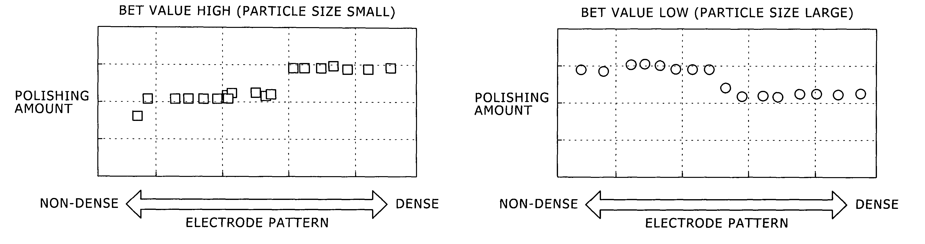
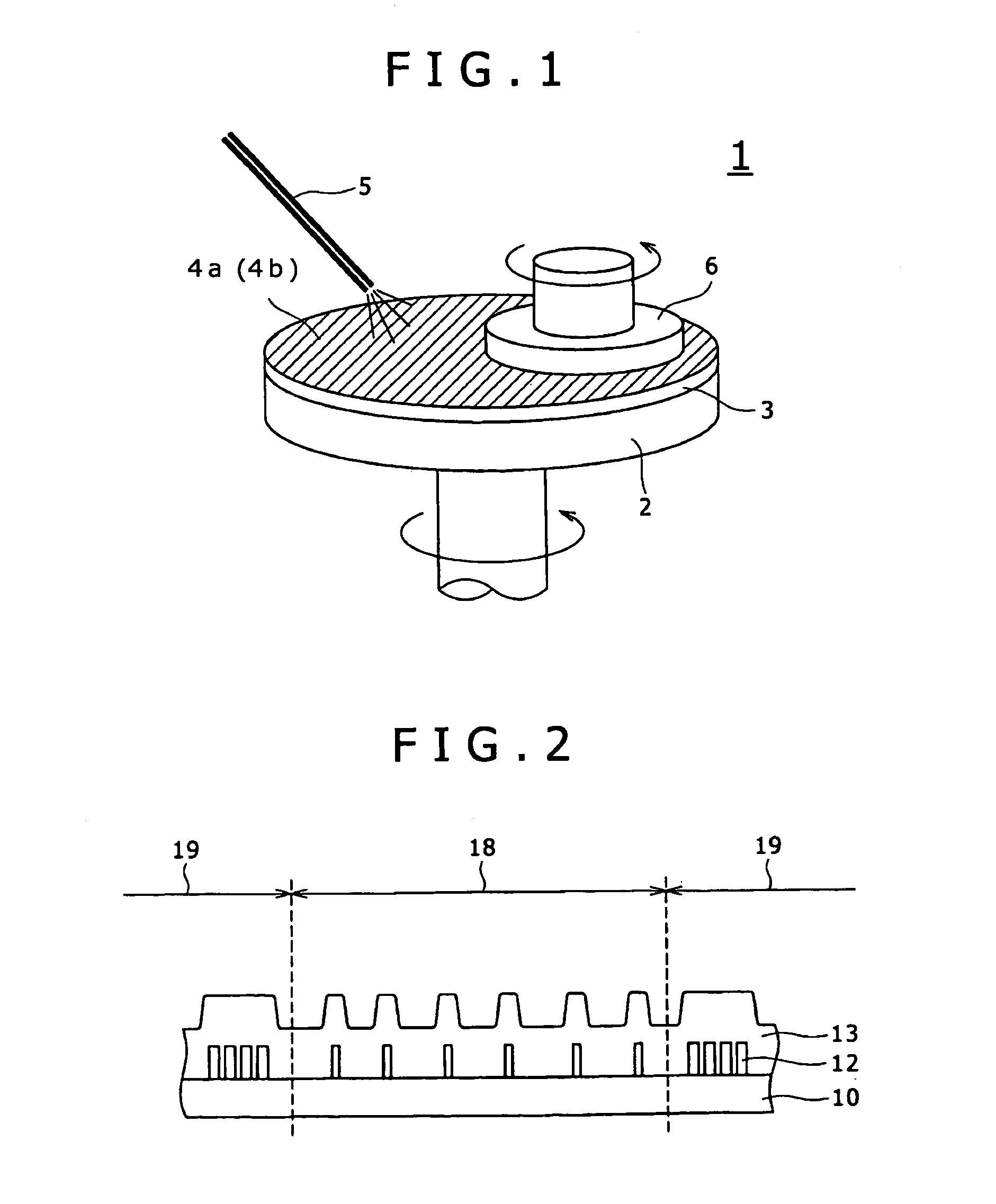
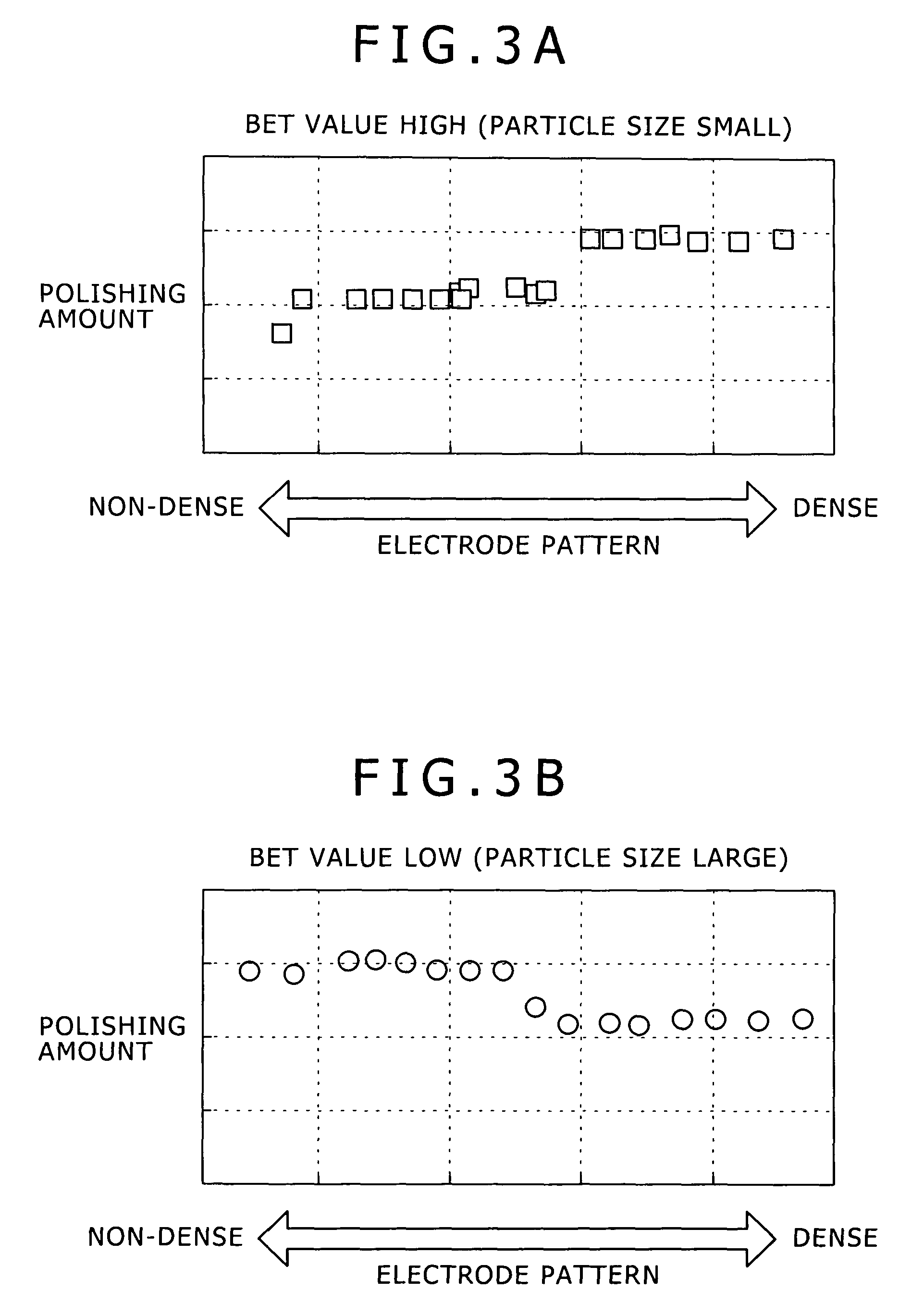
[0029]FIG. 1 shows a general configuration of a polishing apparatus, that is, a CMP apparatus, which is applied to a substrate polishing method according to the present invention. The CMP apparatus is applied to the fabrication of semiconductor devices. Referring to FIG. 1, the CMP apparatus 1 shown is used for CMP processing and includes a surface table 2 having a polishing pad 3 placed on an upper face thereof, a polishing head 6 disposed in an opposing relationship to the surface table 2, and a slurry supplying section 5 for supplying slurries 4a and 4b to the surface of the polishing pad 3.

[0030]The polishing pad 3 may be, for example, a foamed member of a synthetic resin (such as polyurethane) or an abrasive cloth formed from unwoven cloth.

[0031]In a CMP process in which the CMP apparatus of the present embodiment is used, a semiconductor substrate (hereinafter referred to as wafer) (not shown) which may be a silicon wafer, a compound wafer or the like is placed on the surface ...


PUM

PropertyMeasurementUnit
particle sizeaaaaaaaaaa

Abstract

A substrate polishing method, a semiconductor device and a fabrication method for a semiconductor device are disclosed by which high planarization polishing can be achieved. In the substrate polishing method, two or more different slurries formed from ceria abrasive grains having different BET values from each other are used to carry out two or more stages of chemical-mechanical polishing processing of a polishing object oxide film on a substrate to flatten the polishing object film.

Description

CROSS REFERENCES TO RELATED APPLICATIONS[0001]The present invention contains subject matter related to Japanese Patent Application JP 2007-036621 filed in the Japan Patent Office on Feb. 16, 2007, the entire contents of which are incorporated herein by reference.BACKGROUND OF THE INVENTION[0002]1. Field of the Invention[0003]This invention relates to a substrate polishing method, and more particularly, to a substrate polishing method applied to flattening polishing of a polishing object in the form of a thin plate, such as a liquid crystal panel substrate.[0004]The present invention also relates to a semiconductor device fabricated by applying the substrate polishing method and a fabrication method for the semiconductor device.[0005]2. Description of the Related Art[0006]In related art, a colloidal suspension, wherein silicon nitride or a hydrate of silicon nitride is dispersed colloidally or colloidal silica, is used as a polishing agent, that is, as a polishing composition (herein...

Claims


Application Information

Patent Timeline
Patent Type & Authority Patents(United States)
IPC IPC(8): H01L21/302B24B37/00C09G1/02C09K3/14H01L21/304H01L21/3105H01L27/108
CPCH01L21/31053H01L27/10894C09G1/02H10B12/09H01L21/304
Inventor NAKAMURA, HIROKOKOZUKI, TAKAAKIENOMOTO, TAKAYUKIYAMAMOTO, YUICHI
Owner SONY CORP
Why Eureka
Try Eureka