Polishing agent for semiconductor integrated circuit device, polishing method, and method for manufacturing semiconductor integrated circuit device

Inactive Publication Date: 2009-07-09
ASAHI GLASS CO LTD
View PDF7 Cites 1 Cited by
  • Summary
  • Abstract
  • Description
  • Claims
  • Application Information

AI Technical Summary

Benefits of technology

[0019]According to the present invention, when polishing a to-be-polished surface in the production of a semiconductor integrated circuit device, an appropriat

Problems solved by technology

For example, there is a problem that as the refinement of a semiconductor integrated circuit device or multi-layering of wiring advances, convexoconcave (difference in level) on the surface of each layer in the production step becomes great resulting from stacking of layers and exceeds

Method used


Image

  • Polishing agent for semiconductor integrated circuit device, polishing method, and method for manufacturing semiconductor integrated circuit device
  • Polishing agent for semiconductor integrated circuit device, polishing method, and method for manufacturing semiconductor integrated circuit device
  • Polishing agent for semiconductor integrated circuit device, polishing method, and method for manufacturing semiconductor integrated circuit device

Examples


example 1

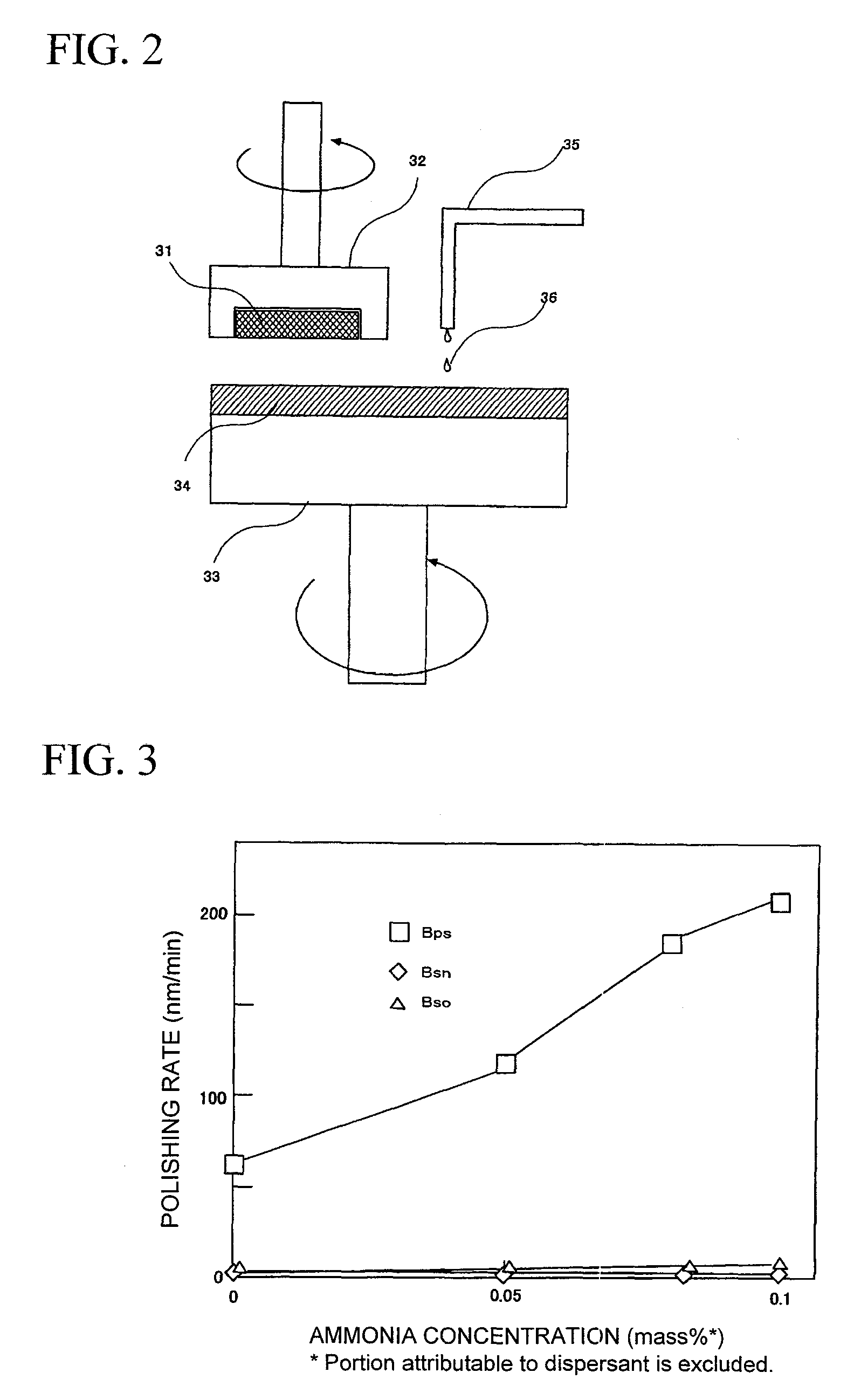
[0080]A cerium oxide abrasive grain and ammonium polyacrylate having a molecular weight of 5,000 as a dispersant were mixed in deionized water with stirring to give a mass ratio of 100:0.7, and the mixture was subjected to ultrasonic dispersion and filtration to obtain a mixture having an abrasive grain concentration of 10% and a dispersant concentration of 0.07%. This mixture vas 5-fold diluted with deionized water to produce Abrasive Grain Mixture A having an abrasive grain concentration of 2.0% and a dispersant concentration of 0.014%. The pH of Abrasive Grain Mixture A was 7.6 and the average particle diameter was 0.19 μm.

[0081]Subsequently, as additives, polyoxypropylene diamine having a molecular weight of 230 (Polyether-Amine, trade name, produced by BASF), which is an amine-based water-soluble polymer, and ammonia which is a basic compound, were dissolved in deionized water to produce Additive Solution B1 having a polyoxypropylene diamine concentration of 2.0% and an ammonia...

example 2

[0084]Abrasive Grain Mixture A was produced in the same manner as in Example 1, and Additive Solution B2 was produced in the same manner as in Example 1 except that in the preparation of Additive Solution B1, the ammonia concentration was adjusted to 0.16%. Additive Solution B2 and Abrasive Grain Mixture A were mixed in a mass ratio of 1:1 to produce a polishing agent having an abrasive grain concentration of 1.0%, a concentration of ammonium polyacrylate as a dispersant of 0.007%, a concentration of polyoxypropylene diamine as an additive of 1.0%, an ammonia concentration of 0.08%, and a pH of 10.9.

[0085]The polishing agent produced was evaluated in the same manner as in Example 1. The composition of the polishing agent and the evaluation results of polishing properties are shown in Table 1.

example 3

[0086]Abrasive Grain Mixture A was produced in the same manner as in Example 1, and Additive Solution B3 was produced in the same manner as in Example 1 except that in the preparation of Additive Solution B1, the ammonia concentration was adjusted to 0.2%. Additive Solution B2 and Abrasive Grain Mixture A were mixed in a mass ratio of 1:1 to produce a polishing agent having an abrasive grain concentration of 1.0%, a concentration of ammonium polyacrylate as a dispersant of 0.007%, a concentration of polyoxypropylene diamine as an additive of 1.0%, an ammonia concentration of 0.1%, and a pH of 10.9.

[0087]The polishing agent produced was evaluated in the same manner as in Example 1. The composition of the polishing agent and the evaluation results of polishing properties are shown in Table 1.


PUM


Abstract

The present invention is to provide a polishing technique ensuring that when polishing a to-be-polished surface in the production of a semiconductor integrated circuit device, appropriate polishing rate ratios can be obtained between a borophosphosilicate glass material layer and other materials and high planarization of the to-be-polished surface containing a borophosphosilicate glass material layer can be thereby realized. The present invention relates to a polishing agent for chemical mechanical polishing, containing a cerium oxide particle, a water-soluble polyamine, one or more basic compounds selected from the group consisting of monoethanolamine, ethylethanolamine, diethanolamine and ammonia, and water, wherein the polishing agent has a pH of from 10 to 13 and wherein the basic compound is contained in an amount of more than 0.01 mass %.

Description

TECHNICAL FIELD[0001]The present invention relates to a polishing technique used in a production step of a semiconductor integrated circuit device. More specifically, the present invention relates to a polishing agent suitable for planarizing a to-be-polished surface containing a borophosphosilicate glass material layer (hereinafter, sometimes referred to as a “BPSG layer”) used in a semiconductor integrated circuit device, and a polishing technique for a BPSG layer-containing to-be-polished surface, used in a production step of a semiconductor integrated circuit device.BACKGROUND ART[0002]With recent progress toward higher integration and higher functionality of a semiconductor integrated circuit device, development of a microfabrication technology for realizing refinement and high density is demanded. In particular, the importance of a planarizing technique by a chemical mechanical polishing method (hereinafter referred to as “CMP”) has been rising.[0003]For example, there is a pr...

Claims


Application Information

Patent Timeline
IPC IPC(8): H01L21/304C09K13/00B24B37/04
CPCB24B37/044H01L21/31053C09K3/1463C09G1/02C09K3/14H01L21/304
Inventor KON, YOSHINORIYOSHIDA, IORINAKAZAWA, NORIHITO
Owner ASAHI GLASS CO LTD
Why Eureka
Try Eureka