Photoelectric conversion device

a conversion device and photoelectric technology, applied in the direction of semiconductor devices, basic electric elements, electrical equipment, etc., can solve the problems of inferior effect to insulating films such as oxide films or nitride films, insufficient conductivity in horizontal directions, light absorption loss, etc., to reduce the effect of carrier recombination in the junction region, the effect of reducing the influence and improving the electric characteristics

Inactive Publication Date: 2015-04-21
SEMICON ENERGY LAB CO LTD
View PDF6 Cites 0 Cited by
  • Summary
  • Abstract
  • Description
  • Claims
  • Application Information

AI Technical Summary

Benefits of technology

[0010]The provision of the i-type amorphous semiconductor layer in a p-n junction region has effects of terminating surface defects of the single crystal silicon substrate and forming a steep junction, which contributes to reduction in carrier recombination at a hetero interface.
[0011]On the other hand, in an amorphous semiconductor layer for forming the junction, there are many localized levels due to many impurities and carrier recombination easily occurs. Further, conduction properties in a horizontal direction are not sufficient because of small electrical conductivity owing to its amorphous structure; thus, a light-transmitting conductive film that promotes movement of carriers is needed over the amorphous semiconductor layer.
[0012]The light-transmitting conductive film can also have an effect of serving as a surface passivation film and an antireflection film; however, the effect is inferior to an insulating film such as an oxide film or a nitride film. Further, light transmittance of the light-transmitting conductive film in a light-absorption wavelength range of a single crystal semiconductor is around 90%, which has been a factor in light absorption loss.
[0013]In view of the above problems, an object of one embodiment of the present invention is to provide a heterojunction type photoelectric conversion device having a structure capable of reducing, carrier recombination in a junction region. Further, another object is to provide a heterojunction type photoelectric conversion device in which electric characteristics are improved by employing a structure without a light-transmitting conductive film.
[0029]According to one embodiment of the present invention, influence, of the carrier recombination in a junction region can be reduced. Further, a heterojunction type photoelectric conversion device can be provided in Which electric characteristics are improved by employing a structure without a light-transmitting conductive film.

Problems solved by technology

Further, conduction properties in a horizontal direction are not sufficient because of small electrical conductivity owing to its amorphous structure; thus, a light-transmitting conductive film that promotes movement of carriers is needed over the amorphous semiconductor layer.
The light-transmitting conductive film can also have an effect of serving as a surface passivation film and an antireflection film; however, the effect is inferior to an insulating film such as an oxide film or a nitride film.
Further, light transmittance of the light-transmitting conductive film in a light-absorption wavelength range of a single crystal semiconductor is around 90%, which has been a factor in light absorption loss.

Method used


Image

  • Photoelectric conversion device
  • Photoelectric conversion device
  • Photoelectric conversion device

Examples


Embodiment Construction

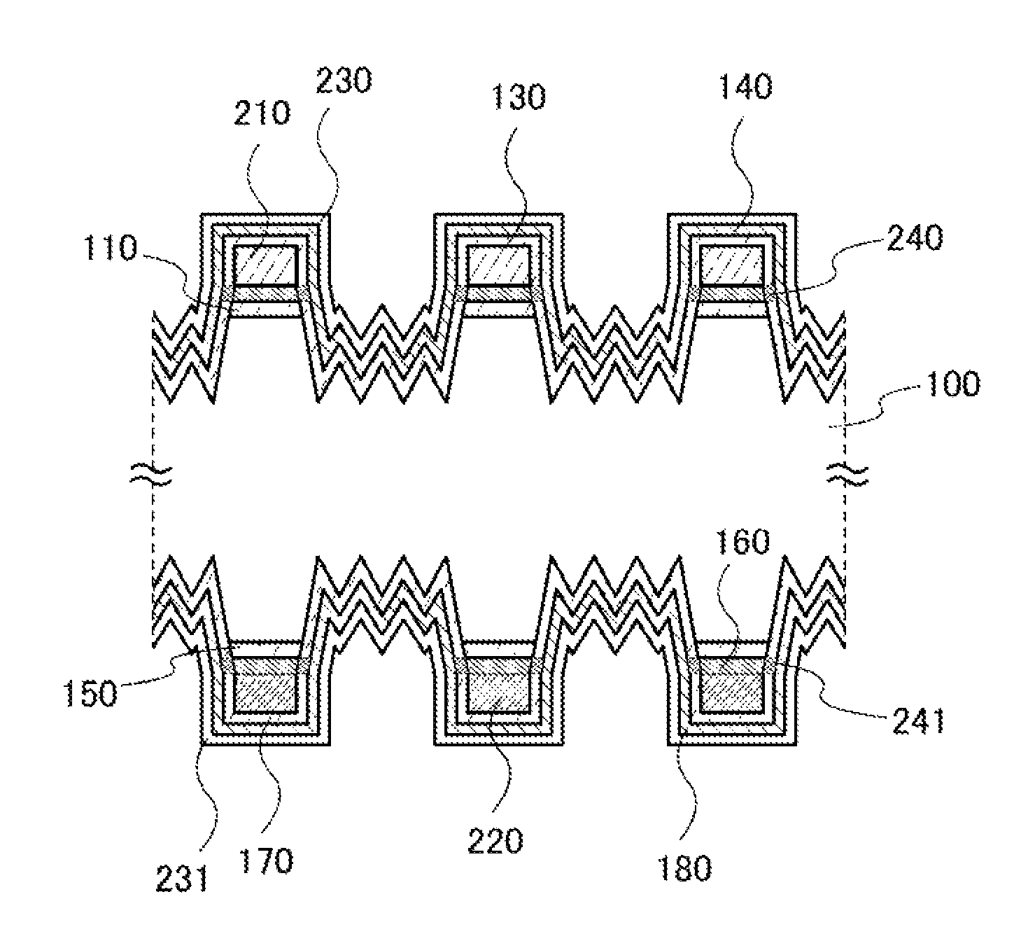
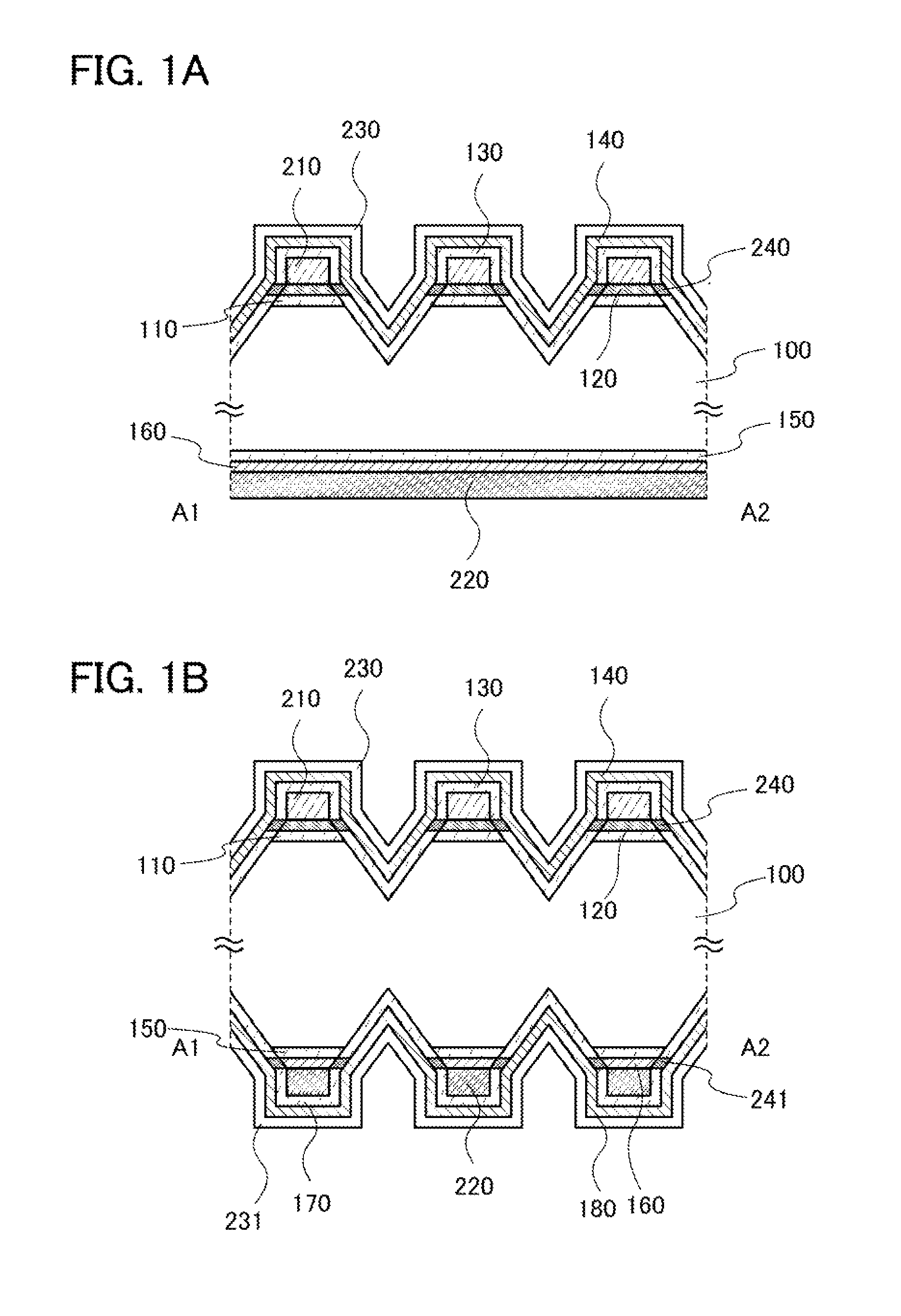
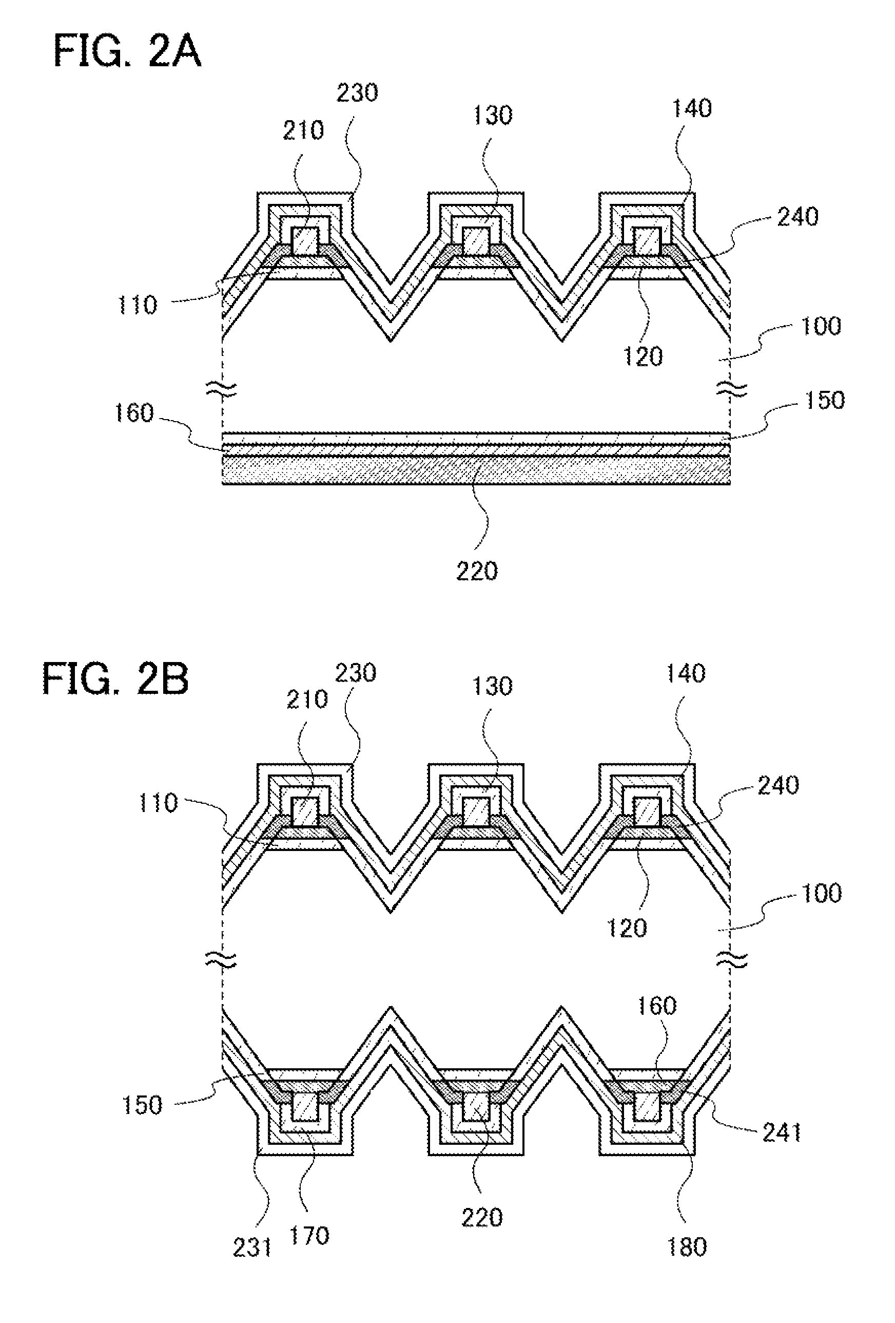
[0037]Hereinafter, embodiments of the present invention will be described in detail with reference to the accompanying drawings. However, the present invention is not limited to the description below, and it is easily understood by those skilled in the art that modes and details disclosed herein can be modified in various ways without departing from the spirit and the scope of the present invention. Therefore, the present invention is not construed as being limited to description of the embodiments. In the drawings for explaining the embodiments, the same portions or portions having similar functions are denoted by the same reference numerals, and description of such portions is not repeated in some cases.

[0038]In this embodiment, a photoelectric conversion device according to one embodiment of the present invention, and a manufacturing method thereof will be described.

[0039]FIGS. 1A and 1B are cross-sectional views each illustrating a photoelectric conversion device according to on...


PUM


Abstract

Provided is a photoelectric conversion device characterized by a lattice-shaped current-collection metal electrode and a depressed portion provided in opening regions of a lattice structured by the lattice-shaped current collection electrode. This structure results in the reduction in the area of a heterojunction containing a highly-doped semiconductor layer, which decreases the influence of carrier recombination promoted by the high concentration of an impurity and leads to the improved electric characteristic of the photoelectric conversion device. The lattice shape of the current collection electrode also makes it possible to exclude the use of a light-transmitting current collection electrode and allows a protective insulating layer having a high light-transmitting property to be formed over the current collection electrode, which contributes to the reduction of the light absorption loss.

Description

BACKGROUND OF THE INVENTION[0001]1. Field of the Invention[0002]The present invention relates to a photoelectric conversion devices.[0003]2. Description of the Related Art[0004]Recently, a photoelectric conversion device that generates power without carbon dioxide emissions has attracted attention as a countermeasure against global warming. As a typical example thereof, a solar cell has been known which uses a crystalline silicon substrate such as a single crystalline substrate or a polycrystalline silicon substrate.[0005]In solar cells using a crystalline silicon substrate, a structure having a so-called homo junction is widely used. In such a structure, a layer having the conductivity type opposite to that of the crystalline silicon substrate is formed on one surface side of the crystalline silicon substrate by diffusion of impurities.[0006]Further, solar cells are disclosed in Patent Documents 1 and 2 in each of which a heterojunction is formed by formation of an amorphous silico...

Claims


Application Information

Patent Timeline
Patent Type & Authority Patents(United States)
IPC IPC(8): H01L31/0236H01L31/0352H01L31/0264H01L31/0224H01L31/0747
CPCH01L31/035281H01L31/022433H01L31/0747Y02E10/547
Inventor YAMAZAKI, SHUNPEI
Owner SEMICON ENERGY LAB CO LTD
Why Eureka
Try Eureka