Semiconductor memory device

a memory device and semiconductor technology, applied in static storage, digital storage, instruments, etc., can solve the problems of excessive write current of pcr element and deterioration of write performance, and achieve the effect of reducing cell manufacturing costs and reducing the minimum manufacturing cost of cells

Active Publication Date: 2015-04-21
SK HYNIX INC
View PDF9 Cites 5 Cited by
  • Summary
  • Abstract
  • Description
  • Claims
  • Application Information

AI Technical Summary

Benefits of technology

[0017]An embodiment of the present invention relates to a semiconductor memory device including a plurality of phase change resistor (PCR) elements that are vertically laminated and coupled in series, resulting in lower manufacturing costs of the cells.
[0018]Another embodiment of the present invention relates to a semiconductor memory device for commonly using one bit line having a vertical structure in a plurality of unit cells sequentially stacked, resulting in minimum manufacturing costs of the cells.

Problems solved by technology

However, a problem of phase change memory (PCM) devices using the PCR element is an excessively high write current for writing data in a cell.
Therefore, the number of cells where data is simultaneously written is limited, such that write performance is deteriorated.

Method used


Image

  • Semiconductor memory device
  • Semiconductor memory device
  • Semiconductor memory device

Examples


Embodiment Construction

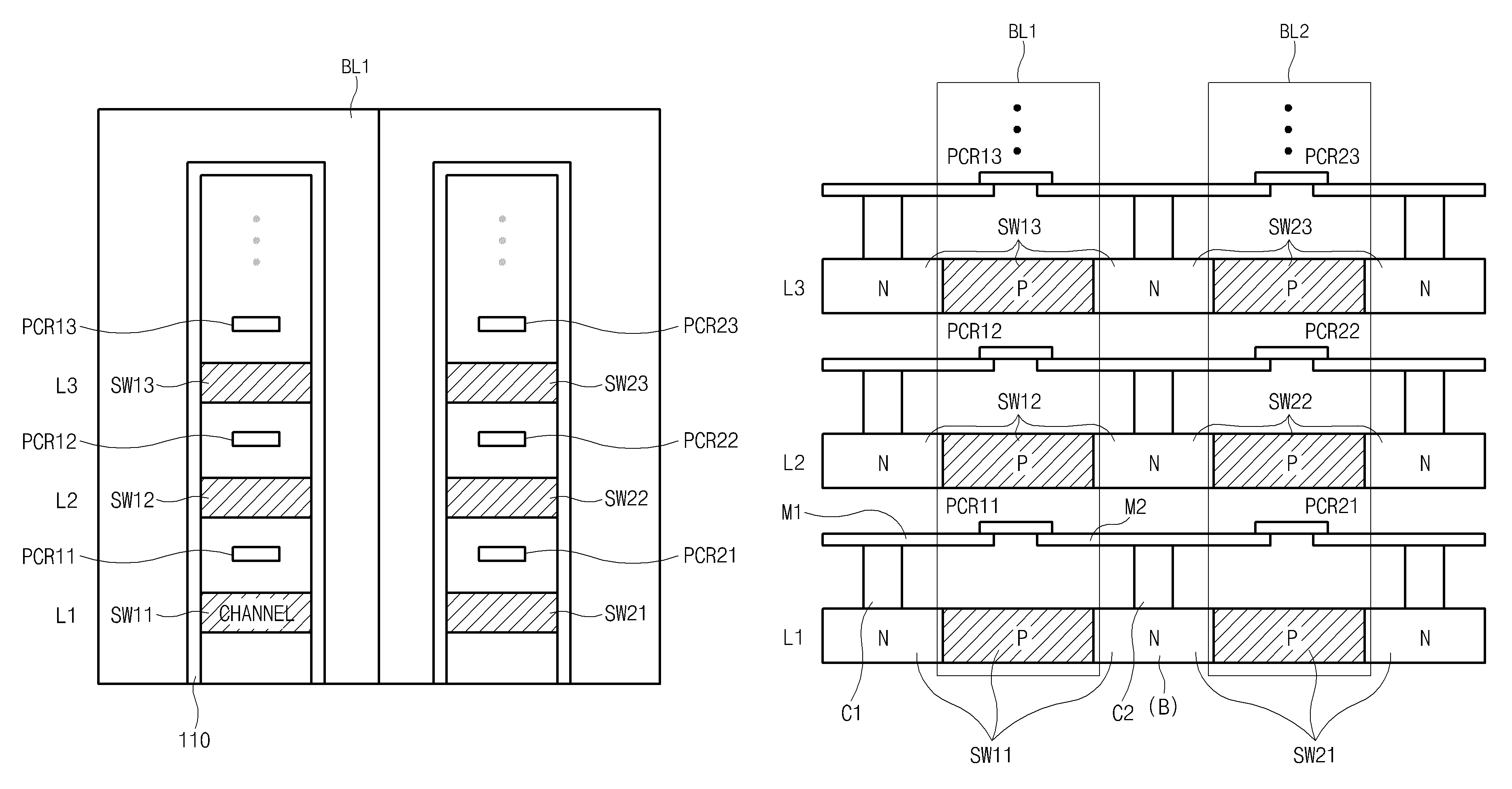
[0037]Reference will now be made in detail to the embodiments of the present invention, examples of which are illustrated in the accompanying drawings. Wherever possible, the same reference numbers will be used throughout the drawings to refer to the same or like parts. A semiconductor memory device according to the present invention will hereinafter be described with reference to the annexed drawings.

[0038]FIG. 4 illustrates a circuit diagram of a semiconductor memory device according to an embodiment of the present invention.

[0039]Referring to FIG. 4, the semiconductor memory device includes a selection switch SW, a plurality of phase change resistor (PCR) elements PCR1˜PCRn, and a plurality of switching elements N1˜Nn. One PCR element and one switching element coupled with the PCR element construct a unit cell.

[0040]The selection switch SW may comprise an NMOS transistor. The selection switch SW is coupled to and disposed between a read / write bit line RWBL and a unit cell UC1, an...


PUM


Abstract

A semiconductor memory device is disclosed, which relates to a technology for a serial cell structure of a phase change memory (PCM). The semiconductor memory device includes a plurality of unit cells stacked with a plurality of layers, and a single bit line formed to have a vertical structure and shared by the plurality of unit cells. Each unit cell includes a switching element including a source region, a drain region, and a channel region, and a phase change resistor (PCR) element formed over the switching element.

Description

CROSS-REFERENCE TO RELATED APPLICATION[0001]The priority of Korean patent application No. 10-2012-0047418 filed on May 4, 2012, the disclosure of which is hereby incorporated in its entirety by reference, is claimed.BACKGROUND OF THE INVENTION[0002]Embodiments of the present invention relate to a semiconductor memory device, and more specifically to a cell structure of a phase change memory (PCM) device, which includes a plurality of vertically laminated unit cells.[0003]Generally, a non-volatile memory device (e.g., a magnetic memory device, a phase change memory (PCM) device, or the like) has a data processing speed similar to that of a volatile random access memory (RAM) device. The non-volatile memory device also preserves data even when power is turned off.[0004]FIGS. 1A and 1B illustrate a conventional phase change resistor (PCR) element 4.[0005]Referring to FIGS. 1A and 1B, the PCR element 4 includes a top electrode 1, a bottom electrode 3, and a phase change material (PCM) l...

Claims


Application Information

Patent Timeline
Patent Type & Authority Patents(United States)
IPC IPC(8): G11C11/00G11C13/00
CPCG11C13/0004G11C2213/71G11C2213/74G11C2213/75G11C2213/79Y10S977/754H10N70/231H10N70/826
Inventor KANG, HEE BOK
Owner SK HYNIX INC
Why Eureka
Try Eureka