

Method for forming layer constituted by repeated stacked layers
a technology of stacked layers and layers, applied in the direction of coatings, metallic material coating processes, chemical vapor deposition coatings, etc., can solve problems such as film separation
- Summary
- Abstract
- Description
- Claims
- Application Information
AI Technical Summary
Benefits of technology
Problems solved by technology
Method used
Image

Examples
example 1
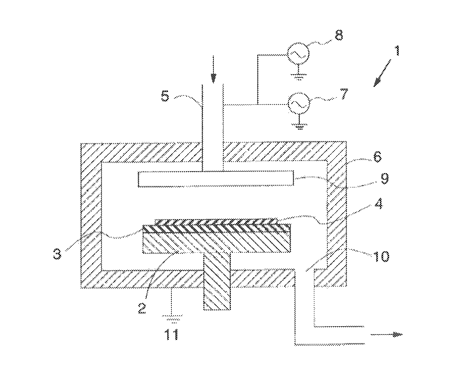
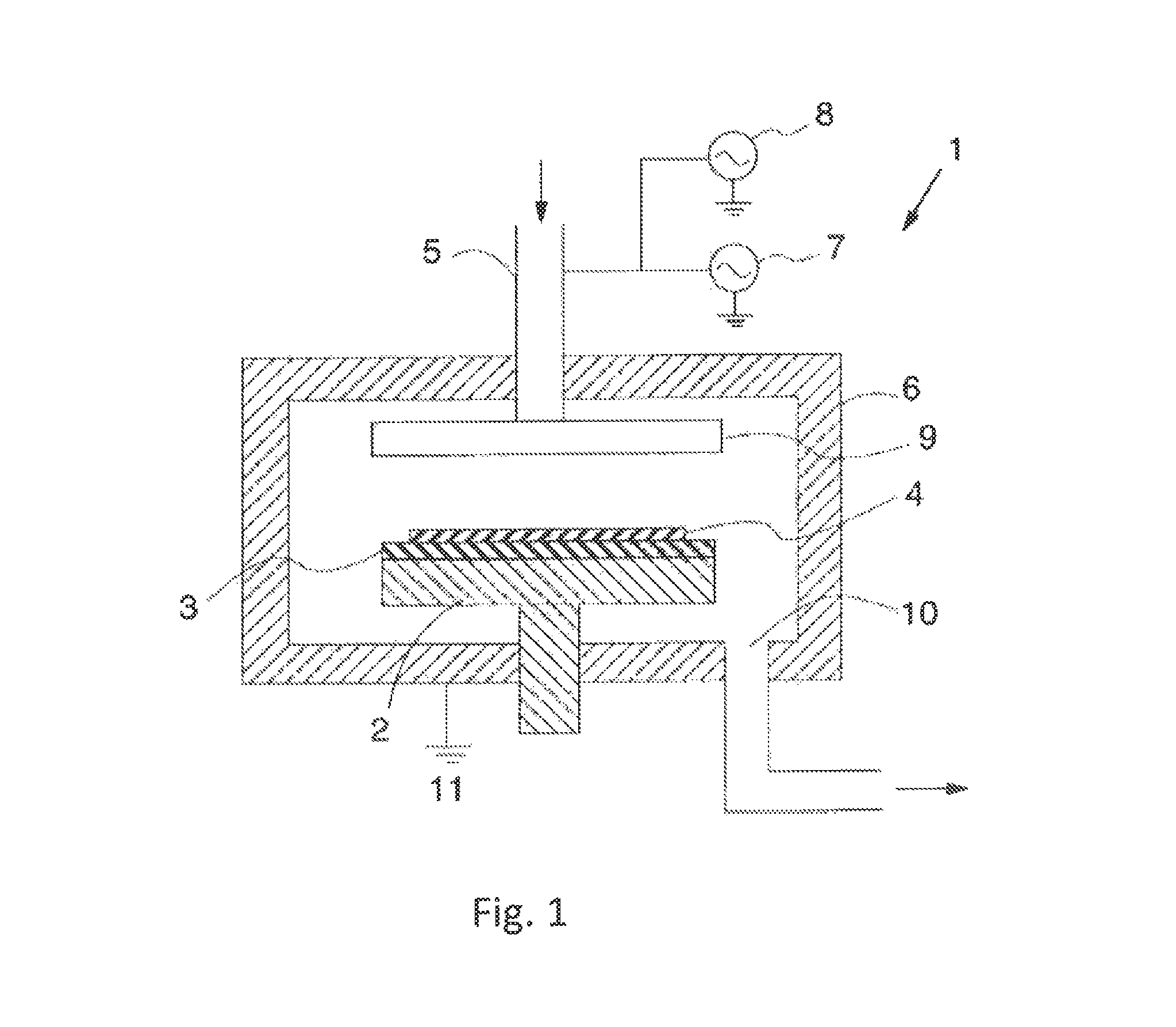
[0042]Thin-film laminates or stacks (repeated stacked layers) consisting of two types of dielectric films were formed on a substrate (having a diameter of 300 mm) by adjusting a flow rate and pressure of each gas and RF power as indicated below using a plasma CVD apparatus illustrated in FIG. 1.
example 1-1
[0043]In this example, SiO was selected as the first dielectric film and SiN, as the second dielectric film. Table 1 shows the process conditions for each film. The conditions here were selected to achieve a stress of around −50 MPa in a stacked state. As shown in Example 1-3, RF power and pressure are the two parameters having strong influence on stress.
[0044]
TABLE 1Process conditions for single layer film and film propertiesFilm PropertyProcess ConditionWetSurfaceSiH4NH3N2ON2Press.RF1RF2SUSStressE / RRoughnessFilm[sccm][sccm][slm][slm][Pa][W][W][° C.][MPa]ratioRRMS (nm)SiO15003.00.0200300100450−1341:2000.4SiN3502000.010.050014000450240.45RF1: 13.56 MHz;RF2: 400 kHz
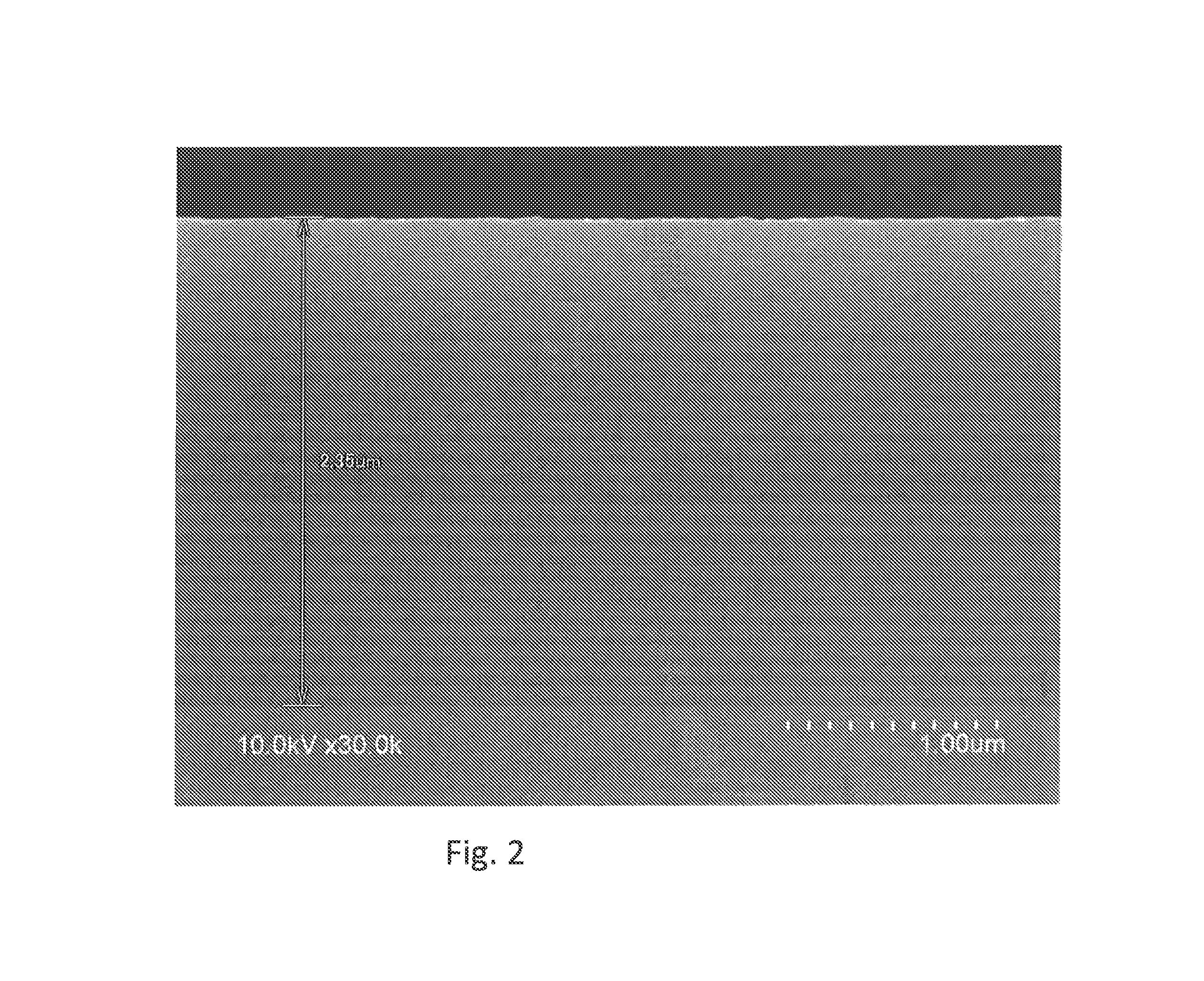
[0045]When a stack was formed by layering 50 nm of each of the films and its stress was measured, a value close to the design, or specifically −45 MPa, was achieved. In addition, the ratio of wet etching rates was 1:200 when hot phosphoric acid was used as the etchant, giving a selectivity of 200. Furthermore, the surface ...
example 1-2
[0048]Next, the 24-stack body obtained above was used to perform evaluation of RIE etching shape according to the evaluation method described below, by making holes under the RIE etching conditions described below. Normally, the bowing shape and tapered shape shown in FIG. 3 are obtained. When films of different types are layered, as is the case here, different etching rates result in a stepped profile. Since the etching rate of the SiO film is slower than the etching rate of the SiN film, SiO remained in the final structure and interpolated the concaved sections to create an appearance of smooth, continuous SiO, and as a result the profile shape shown in FIG. 3 was formed.
[0049]Etching conditions: CF4 200 sccm, O2 50 sccm, RF 800 W, susceptor 30° C., pressure 10 Pa
[0050]Evaluation method: Shape evaluation was conducted according to the calculations described below. The passing condition is roughly W2 / W13 / W1>0.90 for the tapered shape, but W2 / W13 / W1>0.95, for the tapered shape. The ...
PUM
| Property | Measurement | Unit |
|---|---|---|
| frequency | aaaaa | aaaaa |
| temperature | aaaaa | aaaaa |
| thickness | aaaaa | aaaaa |
Abstract
Description
Claims
Application Information