

Semiconductor device and method of manufacturing the same
a semiconductor and device technology, applied in semiconductor devices, capacitors, electrical devices, etc., can solve the problems of increasing leakage current, increasing total capacitance, and blocking the cylindrical hol
- Summary
- Abstract
- Description
- Claims
- Application Information
AI Technical Summary
Benefits of technology
Problems solved by technology
Method used
Image

Examples
example 2
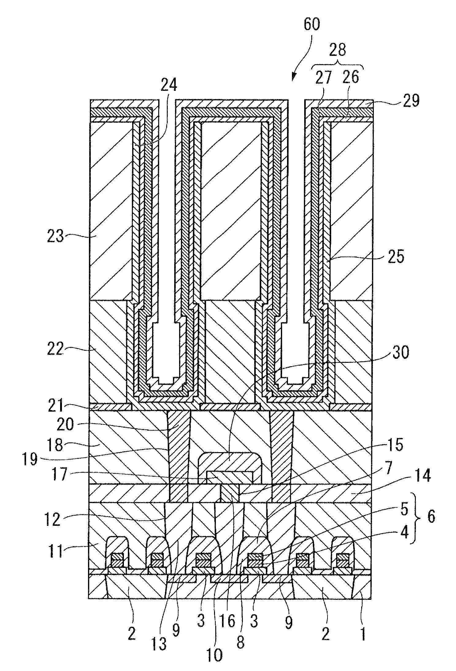
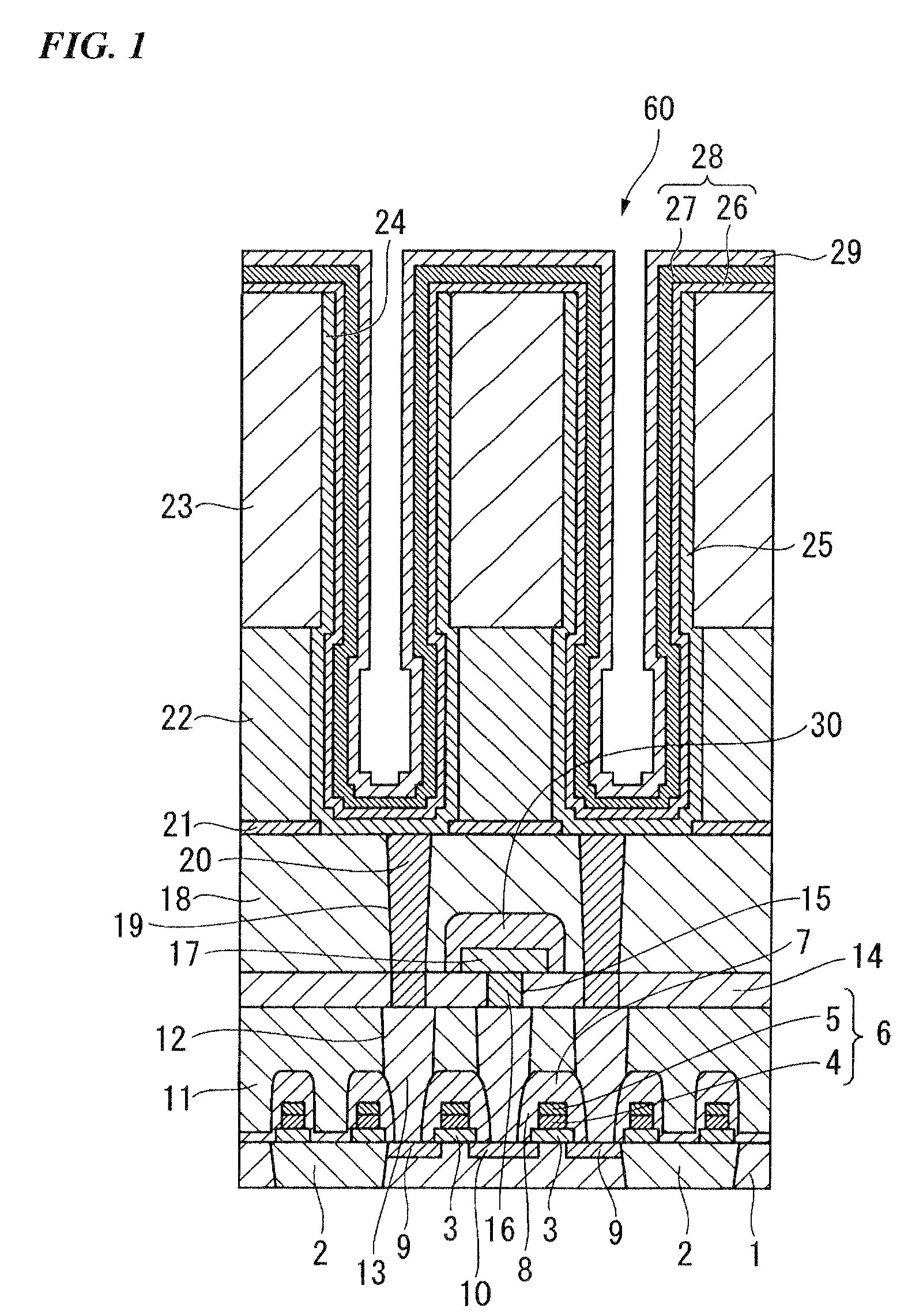
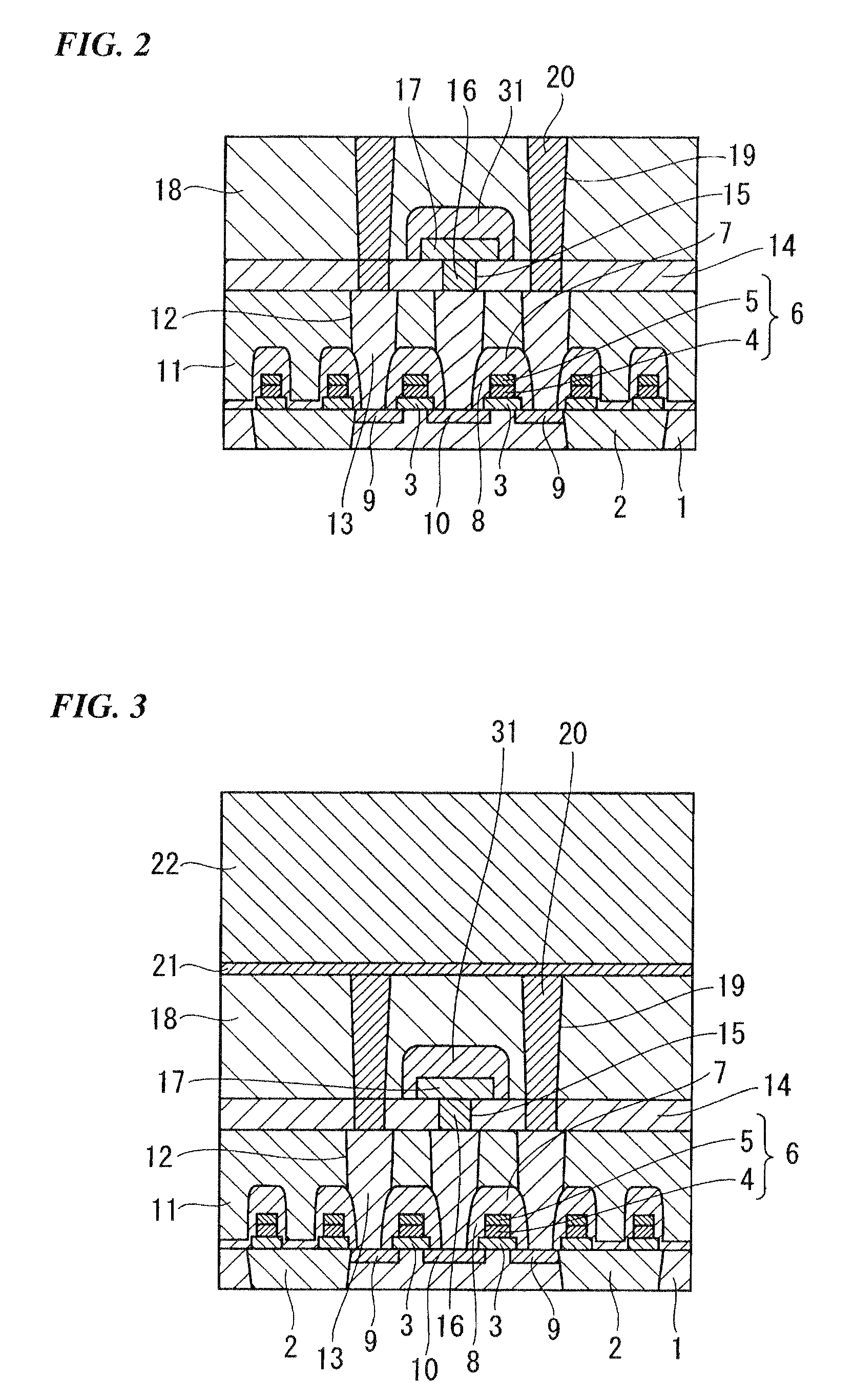
A semiconductor substrate formed with parts up to a capacitor cylinder is prepared using the method and materials according the above-described embodiment. Then, a bottom metal electrode composed of a TiN film is formed in the capacitor cylinder by a CVD method.
Then, using the film forming apparatus shown in FIG. 7, a semiconductor device is manufactured in the same way as Example 1 except that a capacitive insulating film is formed by forming a Si3N4 film (first dielectric layer) having a thickness of 1 nm at a film forming temperature of 550° C. on the bottom metal electrode and its partition using dichlorosilane, ammonia and nitrogen, and forming a ZrO2 film (second dielectric layer) having a thickness of 6 nm at a film forming temperature of 300° C. on the Si3N4 film using TEMAZ (tetrakisethylaminozirconium).
With the above conditions, a semiconductor memory device having a capacitive insulating film composed of the first and second dielectric layers can be obtained. An Ar gas is...
example 3
A semiconductor substrate formed with parts up to a capacitor cylinder is prepared using the method and materials according the above-described embodiment. Then, a bottom metal electrode composed of a TiN film is formed in the capacitor cylinder by a CVD method.
Then, using the film forming apparatus shown in FIG. 7, a semiconductor device is manufactured in the same way as Example 1 except for the conditions that a capacitive insulating film is formed by forming an Al2O3 film (first dielectric layer) having a thickness of 1 nm at a film forming temperature of 300° C. on the bottom metal electrode and its partition using TMA (trimethylaluminum), and forming a HfO2 film (second dielectric layer) having a thickness of 7 nm on the Al3O3 film using TEMAH (tetrakisethylaminohafnium), and an Ru film is formed as an upper metal electrode. An Ar gas is used as a purge gas.
With the above conditions, a semiconductor memory device having a capacitive insulating film composed of the first and se...
example 4
First, a semiconductor substrate formed with parts up to a capacitor cylinder is prepared using the method and materials according the above-described embodiment. Then, a bottom metal electrode composed of an Ru film is formed in the capacitor cylinder by a CVD method.
Then, using the film forming apparatus shown in FIG. 7, a Ta2O5 film (first dielectric layer) having a thickness of 2 nm at a film forming temperature of 300° C. on the bottom metal electrode and its partition using PET (pentaethoxytantalum), and a Ta2O5 film having a thickness of 6 nm is formed at a film forming temperature of 450° C. on the first dielectric layer. An Ar gas is used as a purge gas.
Next, the semiconductor substrate is subjected to an annealing treatment at 450° C. for 10 minutes in a hydrogen atmosphere. Then, an upper metal electrode composed of an Ru film is formed on the capacitive insulating film.
With the above conditions, a semiconductor memory device having a capacitive insulating film composed o...
PUM
| Property | Measurement | Unit |
|---|---|---|
| thickness | aaaaa | aaaaa |
| thickness | aaaaa | aaaaa |
| thickness | aaaaa | aaaaa |
Abstract
Description
Claims
Application Information