Nanometer-scale level structures and fabrication method for digital etching of nanometer-scale level structures

a technology of nanometer-scale level structure and fabrication method, which is applied in the direction of optical elements, instruments, radio frequency controlled devices, etc., can solve the problems of increasing the size, weight and assembly costs of optical systems, adding costs, and challenging fabrication, so as to simplify the fabrication of such systems, reduce the cost of manufacturing, and improve the effect of optical cavity quality

Active Publication Date: 2015-05-19
THE UNITED STATES OF AMERICA AS REPRESENTED BY THE SECRETARY OF THE NAVY
View PDF1 Cites 4 Cited by
  • Summary
  • Abstract
  • Description
  • Claims
  • Application Information

AI Technical Summary

Benefits of technology

[0025]An embodiment of the invention allows micro-fabrication of optically flat steps with nanometer-scale height control with a single lithograph-etch step followed by a chemical etch step. Advantageously, the number of distinct levels achievable is independent from the number of lithograph steps and is independent of the number of resolvable grey-scale lithography levels. This allows for a quite simplified, cost-effective, and time-effective processing sequence.
[0026]An embodiment of the invention significantly simplifies the fabrication of such systems, while ensuring high quality optical cavities for such devices. Furthermore, an embodiment of the invention enables the fabrication of arrays of etalons with more distinct etalon levels than has been previously demonstrated in a single lithography step. Advantageously, in such an embodiment of the invention, the number of distinct etalon levels is limited by the precision of deposition processes (such as atomic layer deposition) rather than the precision of etch rates or pattern transfer.
[0027]An embodiment of the invention has at least three benefits. First, in this embodiment, only one lithograph step (i.e., gray-tone lithography) is required to define the ramp. The individual Etalon levels are made by the chemical etch step. Because only one lithograph step is required, this embodiment of the invention is time and cost effective. Furthermore, the risk of damaging the wafer is reduced because less processing steps are involved. Second, whereas gray-tone lithography alone can produce different levels but the number of distinct gray-levels is limited, the embodiment of the invention has greatly expanded the number of distinct gray-levels that are producible. One could not fabricate 1,000 levels with a gray-mask in a single exposure step. Third, after transferring the gray-scale resist into a dielectric the material surface will be rough; using an etch stop for each etalon leads to optically flat levels.

Problems solved by technology

The requirement of holding imaging optics and dispersive optics in precise alignments adds substantially to the size, weight, and assembly costs of optical systems.
Required tolerances for cavity length can be of nanometer order, making fabrication challenging.
Because each micro-fabrication step is time consuming and adds costs, minimizing the amount of fabrication steps is desired.
The resulting fabrication of a 1,000 level structure by digital etching is quite an effort.

Method used


Image

  • Nanometer-scale level structures and fabrication method for digital etching of nanometer-scale level structures
  • Nanometer-scale level structures and fabrication method for digital etching of nanometer-scale level structures
  • Nanometer-scale level structures and fabrication method for digital etching of nanometer-scale level structures

Examples


Embodiment Construction

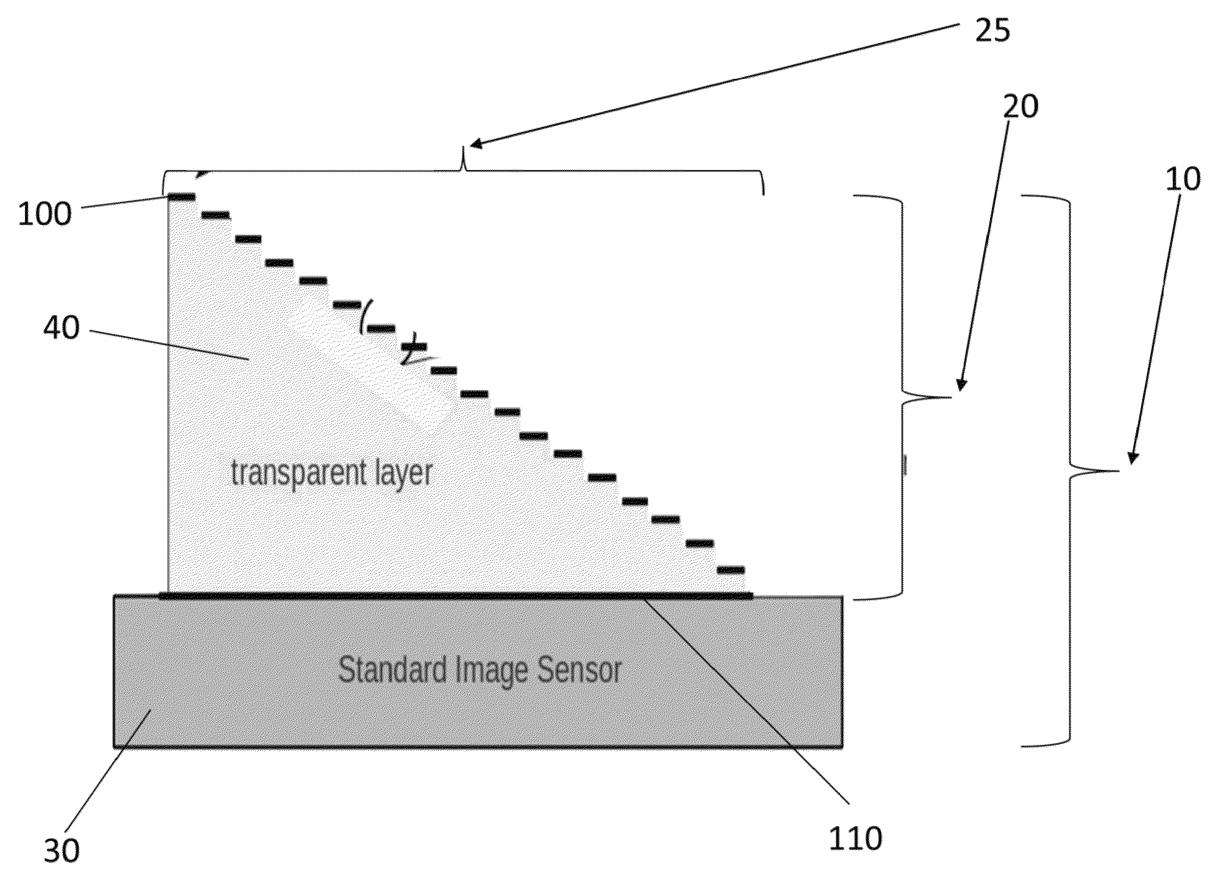
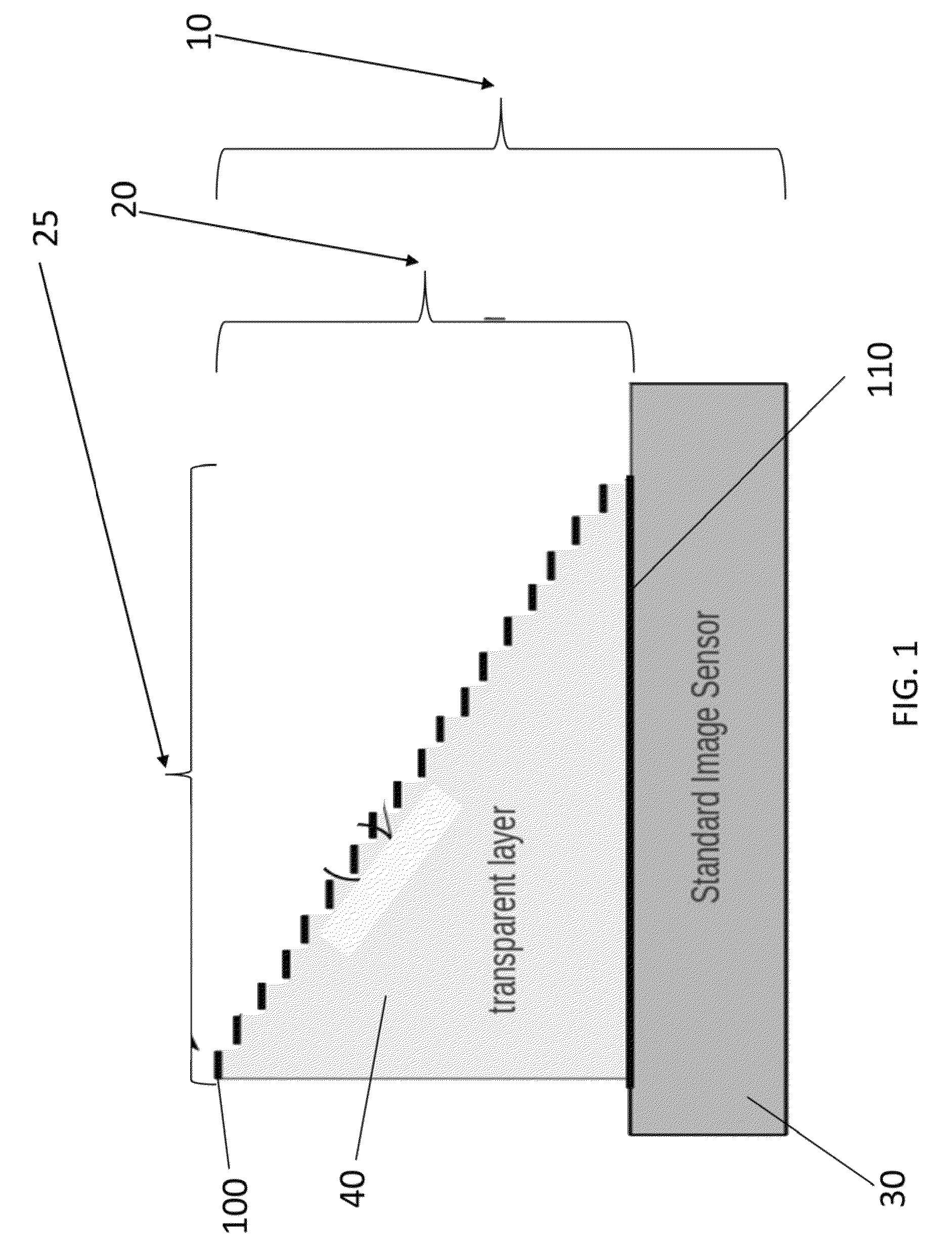
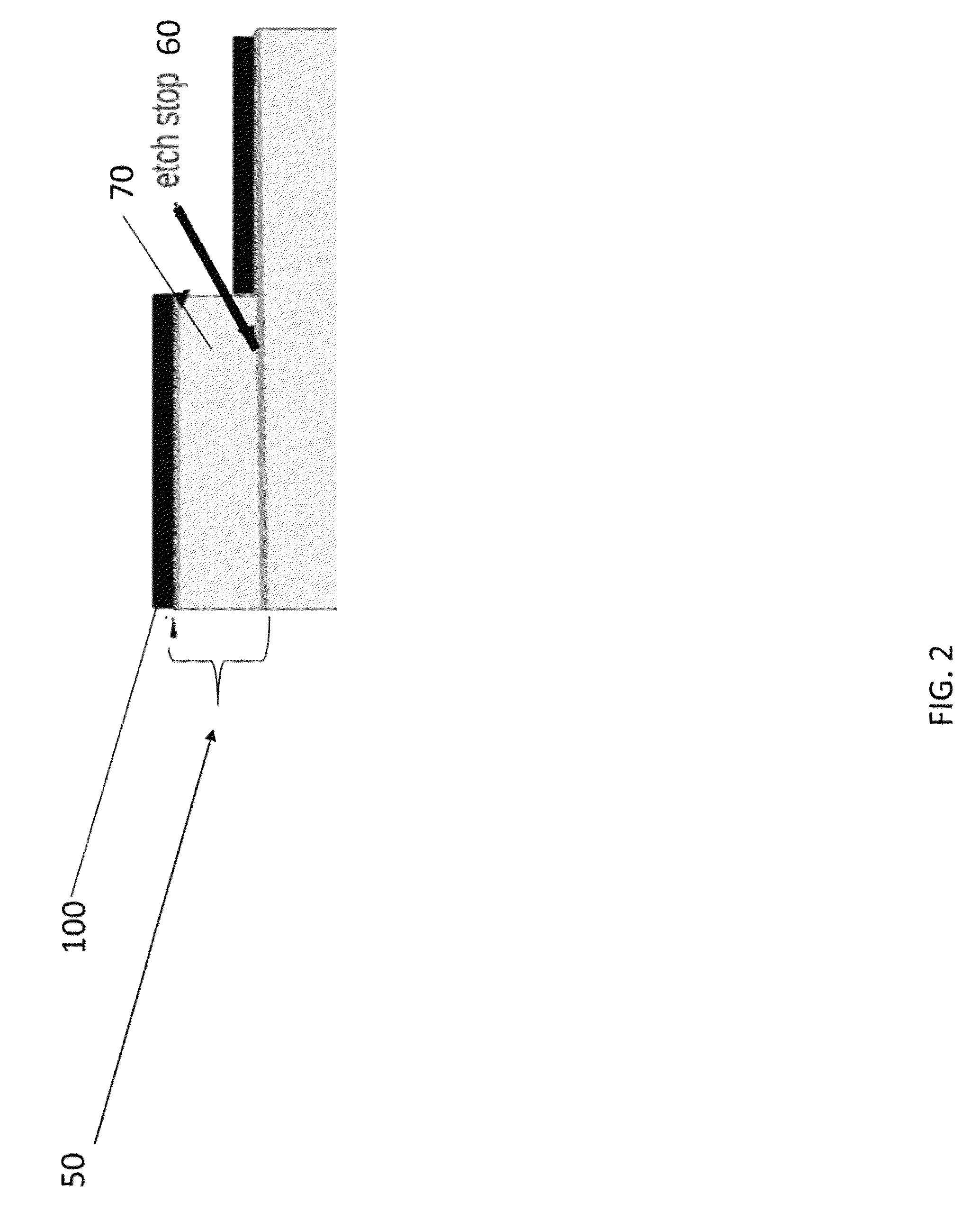
[0037]An embodiment of the invention includes a method of fabricating an integrated optical device 10. The integrated optical device includes a multiple-step structure 20 on a standard substrate 30, as shown in by way of illustration in FIG. 1. A bi-layer stack 40 is deposited in a standard process on the substrate 30, as shown in FIG. 3A. The bi-layer stack 40 includes a plurality of bi-layers, as shown by way of illustration in FIGS. 1 and 2. Each hi-layer 50 of the plurality of bi-layers includes an etch stop layer 60 and a bulk layer 70. The bulk layer 70 is on top of the etch stop layer 60, or vice versa, depending on the application. Standard photoresist 80 is deposited on the bi-layer stack 40, as shown by way of illustration in FIG. 3B. The standard photoresist 80 includes standard negative photoresist or standard positive photoresist. Examples of acceptable standard negative photoresist or standard positive photoresist that are used in gray-tone lithography include DNQ-Novo...


PUM


Abstract

A ramped etalon cavity structure and a method of fabricating same. A bi-layer stack is deposited on a substrate. The bi-layer stack includes a plurality of bi-layers. Each bi-layer of the plurality of bi-layers includes an etch stop layer and a bulk layer. A three dimensional photoresist structure is formed by using gray-tone lithography. The three dimensional photoresist is plasma etched into the bi-layer stack, thereby generating an etched bi-layer stack. The etched bi-layer stack is chemically etched with a first chemical etchant to generate a multiple-step structure on the substrate, wherein the first chemical etchant stops at the etch stop layer.

Description

CROSS-REFERENCE TO RELATED APPLICATIONS[0001]This application claims priority to U.S. Provisional Patent Application Ser. No. 61 / 819,767, entitled “FABRICATION METHOD FOR DIGITAL ETCHING OF NANOMETER-SCALE LEVEL STRUCTURES,” to Boudreau et al., which was filed on 6 May 2013 and is incorporated herein by reference.BACKGROUND OF THE INVENTION[0002]1. Field of the Invention[0003]This invention relates in general to an integrated optical device and method for manufacturing same, and in particular to an integrated optical device having multiple nanometer-scale level structures and method for manufacturing same.[0004]2. Description of the Related Art[0005]Conventional spectrometers typically use dispersive elements to separate light into its spectral components, requiring space and precise alignment of delivery optics. The requirement of holding imaging optics and dispersive optics in precise alignments adds substantially to the size, weight, and assembly costs of optical systems. The siz...

Claims


Application Information

Patent Timeline
Patent Type & Authority Patents(United States)
IPC IPC(8): H01L27/146
CPCH01L27/14629H01L27/14685H01L27/14601H01L27/14683H01L21/31144G01J3/26H01L27/14625G02B6/136G02B6/29358
Inventor BOUDREAU, ANDREW J.YETZBACHER, MICHAEL K.CHRISTOPHERSEN, MARCPHLIPS, BERNARD F.
Owner THE UNITED STATES OF AMERICA AS REPRESENTED BY THE SECRETARY OF THE NAVY
Why Eureka
Try Eureka