

Electro-optical modulator based on carrier depletion or carrier accumulation in semiconductors with advanced electrode configuration
a technology of electrode configuration and electro-optical modulator, which is applied in the field of electro-optical modulators, can solve the problems of reducing signal losses in transmission lines of electro-optical modulators, and cross-talk between neighbouring signal lines of conventional electro-optical modulators of that type, so as to reduce transmission line losses, reduce cross-talk, and reduce the density of on-chip devices
- Summary
- Abstract
- Description
- Claims
- Application Information
AI Technical Summary
Benefits of technology
Problems solved by technology
Method used
Image

Examples
Embodiment Construction
Introduction
[0019]Electro-optical modulators are one of the key components of photonic data transmission systems such as active optical cable transmitters, datacom transmitters or complex quadrature phase shift type transmitters in Metro-Access and Long-Haul telecom networks.
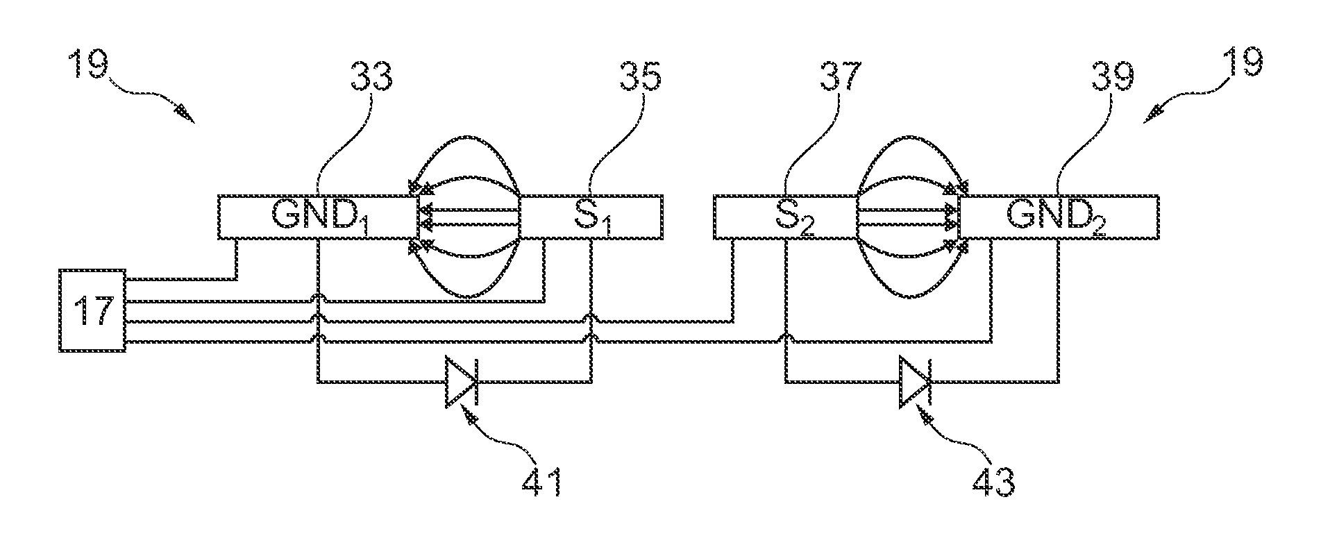
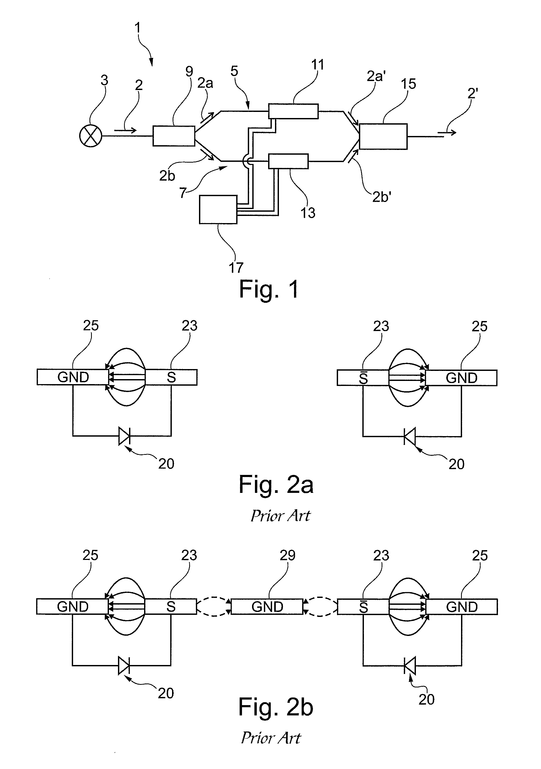
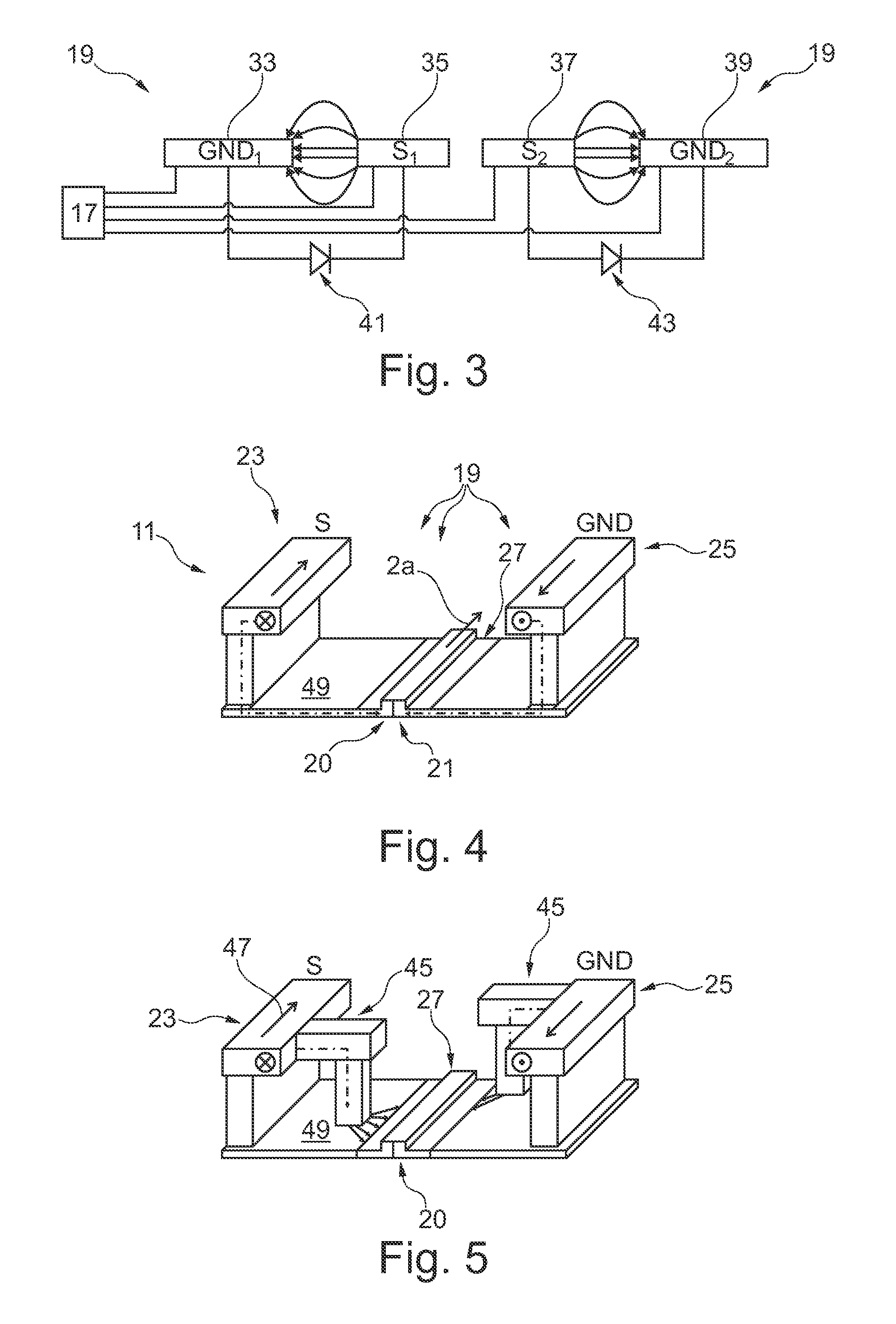
[0020]Embodiments of the invention are generally built on a state-of-the-art depletion type or accumulation type plasma electro-optical modulator 1 based on a Mach-Zehnder interferometer (MZI) architecture in push-pull configuration as schematically depicted in FIG. 1.
[0021]The MZI may be implemented as a waveguide based device that splits incoming light 2 coming from a light source 3 into two modulator-arms 5, 7 using a light splitting device 9 such as a Y-junction splitter (YS), a directional coupler splitter (DCS) or a multimode-interferometer (MMI). In both of the modulator-arms 5, 7 an electrically driven phase modulator 11, 13 is implemented that is adapted to tune the phase velocity of the propagating lig...
PUM
| Property | Measurement | Unit |
|---|---|---|
| frequencies | aaaaa | aaaaa |
| frequency | aaaaa | aaaaa |
| RF frequencies | aaaaa | aaaaa |
Abstract
Description
Claims
Application Information