

Developer for photosensitive resist material and patterning process
a technology of resist film and development process, which is applied in the field of development of photosensitive resist film and patterning process, can solve the problems of acid diffusion, image blur, and inability to achieve the effect of reducing throughput, preventing pattern collapse or bridge defect formation, and suppressing resist film swell during developmen
Active Publication Date: 2015-06-09
SHIN ETSU CHEM CO LTD
View PDF18 Cites 3 Cited by
- Summary
- Abstract
- Description
- Claims
- Application Information
AI Technical Summary
Benefits of technology
Problems solved by technology
It becomes of concern that a dimensional error of a mask has an impact on the dimensional variation of a pattern on wafer.
Since the mask exposure tool is designed for exposure by direct continuous writing, a lowering of sensitivity of resist film leads to an undesirably reduced throughput.
As the feature size is reduced, image blurs due to acid diffusion become a problem.
Since chemically amplified resist compositions are designed such that sensitivity and contrast are enhanced by acid diffusion, an attempt to minimize acid diffusion by reducing the temperature and / or time of post-exposure baking (PEB) fails, resulting in drastic reductions of sensitivity and contrast.
One serious problem in the EUV lithography is pattern collapse.
Method used
View moreImage
Smart ImageViewing Examples

Examples
example
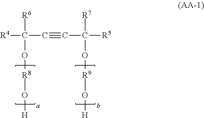
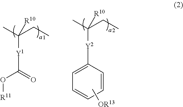
[0172]Examples and Comparative Examples are given below for further illustrating the invention, but they should not be construed as limiting the invention thereto. Mw is a weight average molecular weight as measured by GPC versus polystyrene standards, and Mw / Mn designates molecular weight distribution or dispersity. All parts (pbw) are by weight.
Login to View More PUM
| Property | Measurement | Unit |
|---|---|---|
| wavelength | aaaaa | aaaaa |
| wavelength | aaaaa | aaaaa |
| wavelength | aaaaa | aaaaa |
Abstract
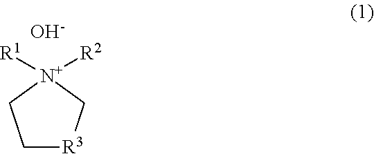
An aqueous solution containing 0.1-20 wt % of a cyclic ammonium hydroxide is a useful developer for photosensitive resist materials. A resist pattern is formed by applying a chemically amplified positive resist composition onto a substrate to form a resist film, exposing the resist film to high-energy radiation, and developing the exposed resist film in a cyclic ammonium hydroxide-containing aqueous solution.
Description
CROSS-REFERENCE TO RELATED APPLICATION[0001]This non-provisional application claims priority under 35 U.S.C. §119(a) on Patent Application No. 2013-123335 filed in Japan on Jun. 12, 2013, the entire contents of which are hereby incorporated by reference.TECHNICAL FIELD[0002]This invention relates to a developer for photosensitive resist materials and a patterning process using the same.BACKGROUND ART[0003]To meet the demand for higher integration density and operating speed of LSIs, the effort to reduce the pattern rule is in rapid progress. The wide-spreading flash memory market and the demand for increased storage capacities drive forward the miniaturization technology. As the advanced miniaturization technology, manufacturing of microelectronic devices at the 65-nm node by the ArF lithography has been implemented in a mass scale. Manufacturing of 45-nm node devices by the next generation ArF immersion lithography is approaching to the verge of high-volume application. The candida...
Claims
Login to View More Application Information
Patent Timeline
 Patent Type & AuthorityPatents(United States)
IPC IPC(8): G03F7/32G03F7/38G03F7/26G03F7/20
CPCG03F7/32G03F7/26G03F7/38G03F7/322G03F7/2037G03F7/2039G03F7/2053G03F7/2065G03F7/2059G03F7/0045G03F7/0046G03F7/0397C08F2/48G03F7/0381G03F7/0392H01L21/0273
InventorHATAKEYAMA, JUNOHASHI, MASAKI
OwnerSHIN ETSU CHEM CO LTD