Semiconductor device

a technology of semiconductors and transistors, applied in the direction of semiconductor devices, basic electric elements, electrical equipment, etc., can solve the problems of high-speed switching characteristics of devices, increased capacitance between the gate electrode and the emitter electrode, and deterioration of switching characteristics, so as to improve the turn-on characteristics, reduce yield, and increase the number of process steps

Active Publication Date: 2015-06-09
FUJI ELECTRIC CO LTD
View PDF19 Cites 3 Cited by
  • Summary
  • Abstract
  • Description
  • Claims
  • Application Information

AI Technical Summary

Benefits of technology

[0023]The present invention has been made in view of the above-mentioned problems. It provides a semiconductor device which can improve turn-on characteristics, such as an on-voltage when the semiconductor device is turned on and switching loss, with a slight increase in the number of process steps, while preventing an increase in costs and a reduction in yield.
[0033]According to the semiconductor device of the invention, it is possible to improve turn-on characteristics, such as switching loss and an on-voltage when the semiconductor device is turned on, with a slight increase in the number of process steps, while preventing an increase in costs and a reduction in yield.

Problems solved by technology

However, the power device requires high-speed switching characteristics in addition to a low on-voltage and an important challenge is to improve the characteristics.
However, in the trench gate IGBT and the IEGT, as the density of the trench structure increases in order to reduce the on-voltage, the capacitance between the gate electrode and the emitter electrode increases and the switching characteristics deteriorate.
As a result, the switching characteristics deteriorate and switching loss increases.
In addition, the total loss of the power device is the sum of steady loss which is determined by the on-voltage and the switching loss which occurs during a switching operation.
Therefore, the number of process steps is too large and there is a concern that costs will increase or yield will be reduced.

Method used


Image

  • Semiconductor device
  • Semiconductor device
  • Semiconductor device

Examples


embodiment 1

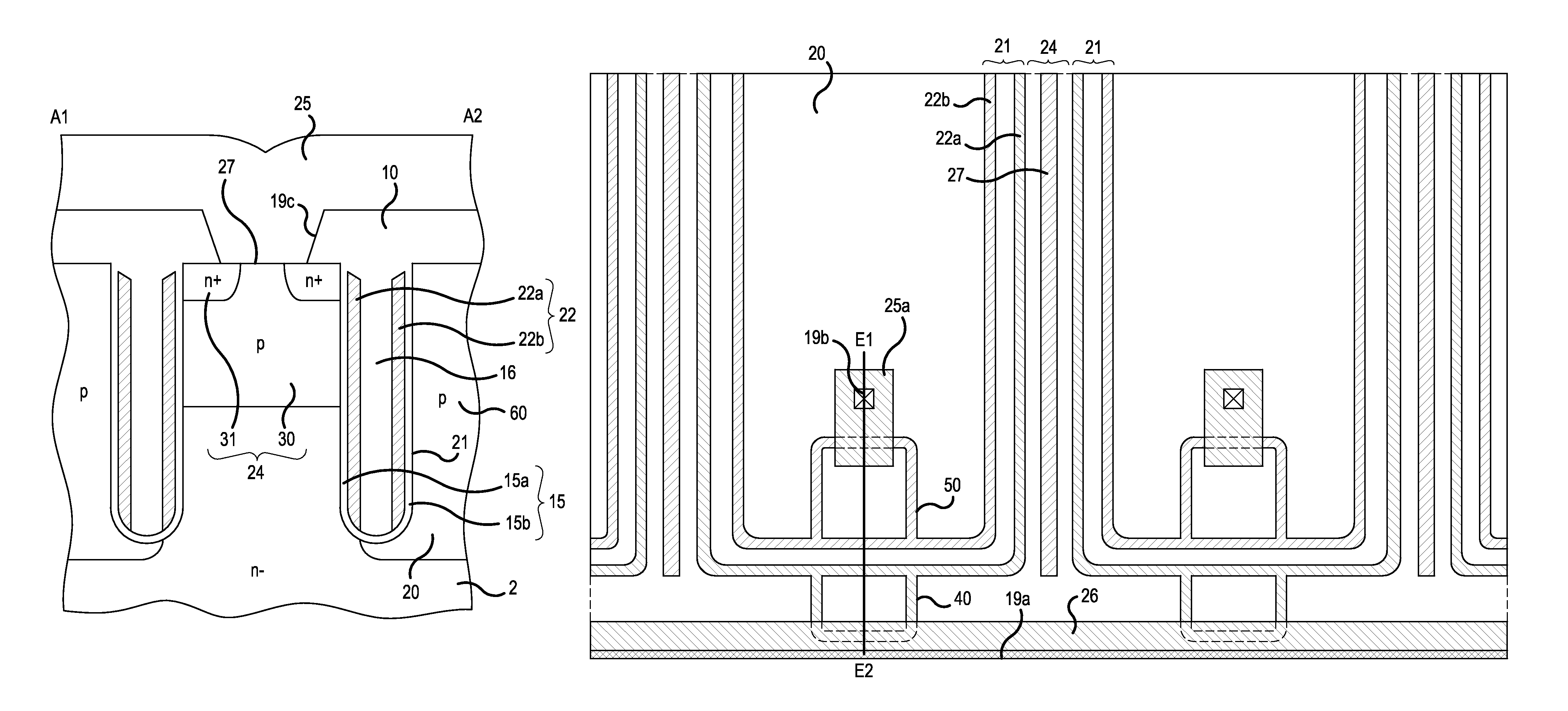
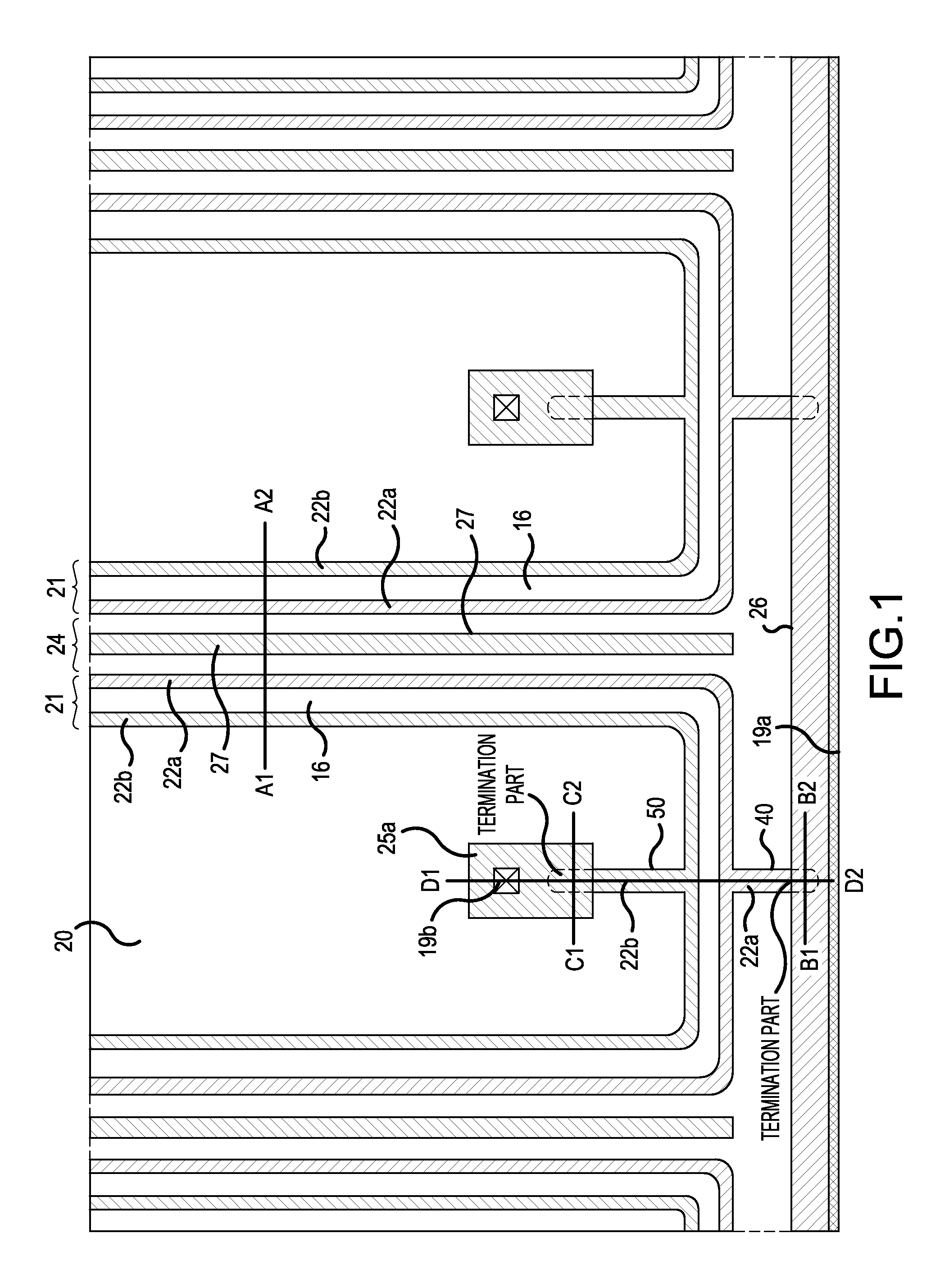
[0053]The structure of a semiconductor device according to Embodiment 1 will be described. FIG. 1 is a plan view illustrating the planar layout of a main portion of the semiconductor device according to Embodiment 1. FIG. 9 is a cross-sectional view illustrating a cross-sectional structure taken along the cutting line A1-A2 of FIG. 1. FIG. 10 is a cross-sectional view illustrating a cross-sectional structure taken along the cutting lines B1-B2 and C1-C2 of FIG. 1. FIG. 11 is a cross-sectional view illustrating a cross-sectional structure taken along the cutting line D1-D2 of FIG. 1. First, the planar layout of the semiconductor device according to Embodiment 1 will be described. The semiconductor device according to Embodiment 1 includes an active region in which a current flows in an on state and a breakdown voltage region which reduces the electric field of a portion of an n− drift layer which is close to a front surface of a silicon substrate and holds a breakdown voltage. The br...

embodiment 2

[0089]Next, the structure of a semiconductor device according to Embodiment 2 will be described. FIG. 12 is a plan view illustrating the planar layout of a main portion of the semiconductor device according to Embodiment 2. The semiconductor device according to Embodiment 2 differs from the semiconductor device according to Embodiment 1 in the planar shape of the second and third trenches 40 and 50. Specifically, as shown in FIG. 12, the second trench 40 has a substantial U-shape in a plan view and both ends thereof are connected to the outer side wall of the first trench 21. That is, the second trench 40 and a portion of the first trench 21 form a substantially rectangular ring shape in a plan view. The planar shape of the second trench 40 is not limited to the substantial U-shape. The second trench 40 may be formed such that both ends thereof are connected to the outer side wall of the first trench 21 to form a substantially rectangular ring shape in a plan view together with the ...

embodiment 3

[0095]FIG. 14 is a plan view illustrating the planar layout of a main portion of a semiconductor device according to Embodiment 3. The semiconductor device according to Embodiment 3 differs from the semiconductor device according to Embodiment 1 in the number of second trenches 40 with respect to one third trench 50 and the position of the second trench 40. Specifically, in Embodiment 1, the second trench 40 faces the third trench 50 with the first trench 21 interposed therebetween. More specifically, the second trench 40 and the third trench 50 are arranged on the same straight line which traverses the first trench 21. In contrast, in Embodiment 3, as shown in FIG. 14, two second trenches 40 are arranged with respect to one third trench 50, and the second trench 40 and the third trench 50 do not directly face each other, with the first trench 21 interposed therebetween. Specifically, for example, a plurality of second trenches 40 are provided with respect to one third trench 50 and...


PUM


Abstract

A semiconductor device includes a first gate electrode that is provided on a first insulating film along one side wall of a first trench and is provided in a second trench, a shield electrode that is provided on a second insulating film along the other side wall of the first trench and is provided in a third trench, a gate runner that is an extended portion of the second trench, has a portion which is provided on the first gate electrode, and is connected to the first gate electrode, and an emitter polysilicon layer that is an extended portion of the third trench, has a portion which is provided on the shield electrode, and is connected to the shield electrode. The semiconductor device has improved turn-on characteristics with a slight increase in the number of process steps, while preventing increase in costs and reduction in yield.

Description

BACKGROUND OF THE INVENTION[0001]A. Field of the Invention[0002]The present invention relates to a semiconductor device, and more particularly, to a trench gate insulated gate bipolar transistor (IGBT).[0003]B. Description of the Related Art[0004]A technique for reducing the power consumption of a power conversion device has been developed and there are great expectations for a technique for reducing the power consumption of a power device which plays a central role in the power conversion device. Among the power devices, an insulated gate bipolar transistor (IGBT) which can reduce an on-voltage using a conductivity modulation effect and is easily controlled by the control of a voltage-driven gate is generally used.[0005]As a MOS gate (an insulated gate with a metal-oxide-semiconductor structure) structure of the IGBT, the following have been known: a planar gate IGBT in which a gate electrode is provided along the surface of a wafer, and a trench gate IGBT in which a polysilicon ga...

Claims


Application Information

Patent Timeline
Patent Type & Authority Patents(United States)
IPC IPC(8): H01L29/739H01L29/423H01L29/66H01L29/10H01L29/417H01L29/49
CPCH01L29/7397H01L29/4236H01L29/4238H01L29/66348H01L29/1095H01L29/41708H01L29/42304H01L29/4916H01L29/407H01L29/7811H01L29/7813H01L29/0619
Inventor ONOZAWA, YUICHITAKAHASHI, HIDENORIYOSHIMURA, TAKASHI
Owner FUJI ELECTRIC CO LTD
Why Eureka
Try Eureka