Switching power supply device, switching power supply circuit, and electrical equipment

a switching power supply circuit and power supply device technology, applied in the direction of electric variable regulation, process and machine control, instruments, etc., can solve the problems of complicated circuit configuration, difficult downsizing, and difficulty in reducing power supply capacity, so as to facilitate downsizing and reduce power supply capacity , the effect of increasing packaging density

Inactive Publication Date: 2015-06-30
TOSHIBA LIGHTING & TECH CORP
View PDF17 Cites 1 Cited by
  • Summary
  • Abstract
  • Description
  • Claims
  • Application Information

AI Technical Summary

Benefits of technology

[0017]The object of an embodiment of the invention is to provide a switching power supply device and a switching power supply circuit which are able to perform turn-off control of the switching element without using the resistance element for current detection, can be adapted to a switching power supply of diverse circuit configurations, and furthermore achieve significant downsizing of the switching power supply.
[0018]The object of the embodiment of the invention is to provide an electrical equipment including the switching power supply device or the switching power supply circuit. The switching power supply device facilitates downsizing by increasing packaging density and reduces electromagnetic interference between mounted circuit components.Solution to Problem

Problems solved by technology

However, when the switching power supply is operated at high frequency of MHz or more, for example, 10 MHz or more using wide bandgap semiconductor, difficulty is involved on following points.(1) because of difficulty in achieving an oscillator responsive to high frequency, not adequate to control by separate excitation control.(2) difficult in control at high frequency.(3) influence of interconnect and structural impedance involved in high frequency operation is increased and operation is influenced.
Therefore, circuit configuration is complicated and furthermore downsizing becomes difficult.
Here, by high frequency operation, the noise component emitted from the mounted device increases to cause electromagnetic interference between circuit elements.
Thus, a problem is to reduce this electromagnetic interference while maintaining downsizing.
Furthermore, in addition to the above problem, the downsizing involves significant temperature increase of circuit parts such as the switching element due to the heat generated from the circuit parts.

Method used


Image

  • Switching power supply device, switching power supply circuit, and electrical equipment
  • Switching power supply device, switching power supply circuit, and electrical equipment
  • Switching power supply device, switching power supply circuit, and electrical equipment

Examples


first embodiment

[0043]First, a first embodiment is described.

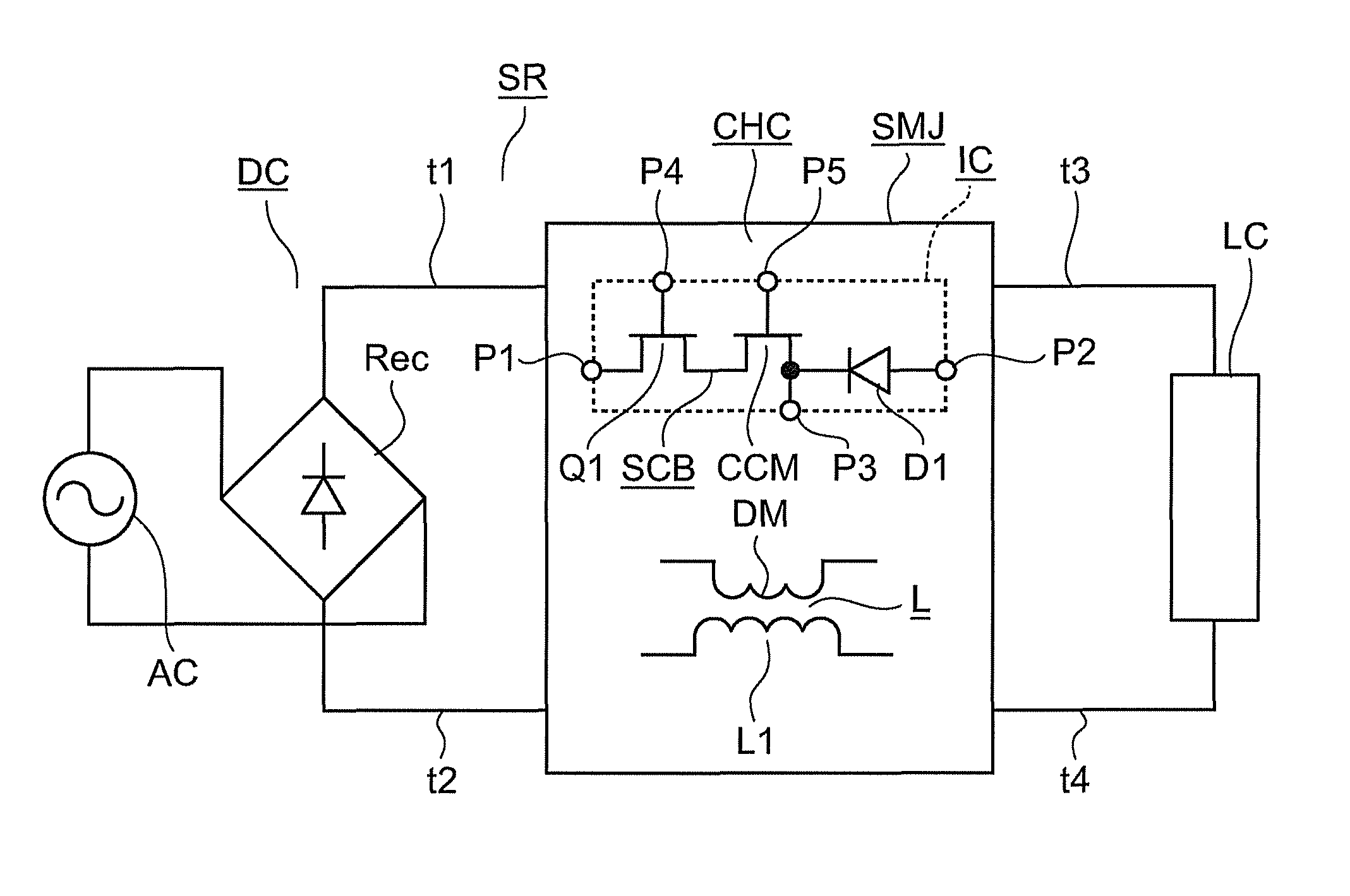
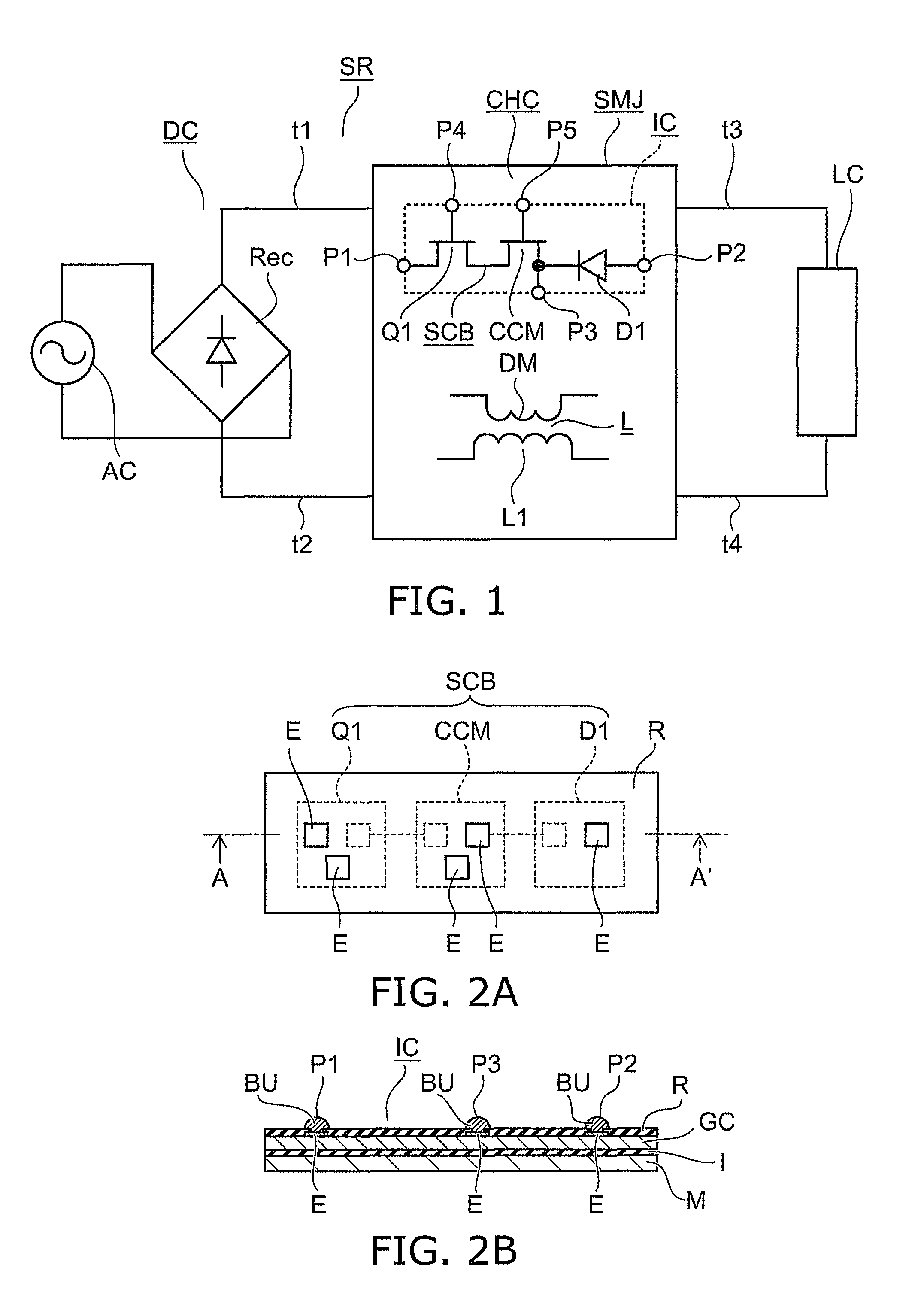
[0044]FIG. 1 is a circuit diagram illustrating a switching power supply device according to the first embodiment.

[0045]FIGS. 2A and 2B illustrate the configuration of the switching power supply device. More specifically, FIG. 2A is a schematic top view, and FIG. 2B is a sectional view taken along line A-A′ of FIG. 2A.

[0046]As shown in FIGS. 1 to 2B, the switching power supply device IC according to the first embodiment includes an integrated body SCB in which a first switching element Q1, a constant current element CCM, and a diode D1 are connected in series and integrated. Furthermore, the switching power supply device IC includes first to fifth external terminals P1-P5 as a plurality of external terminals. The first external terminal P1 is connected to the main terminal of the element disposed on one end side of the integrated body SCB. The second external terminal P2 is connected to the main terminal of the element disposed on the othe...

second embodiment

[0065]A second embodiment is described.

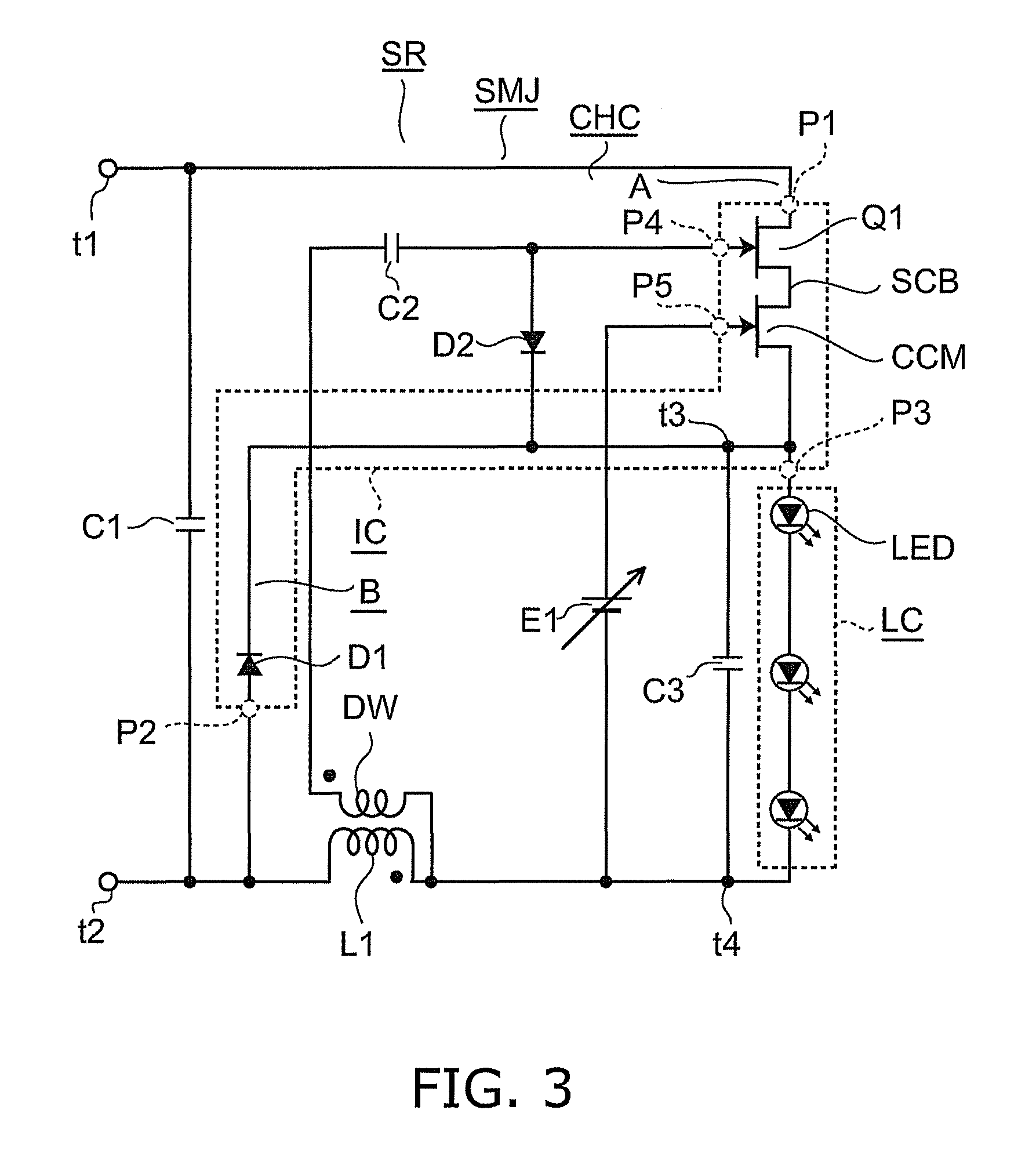
[0066]FIG. 3 is a circuit diagram illustrating a switching power supply circuit according to the second embodiment.

[0067]As shown in FIG. 3, the chopper circuit CHC is of the step-down type. For each of the first switching element Q1 and the constant current element CCM of its switching power supply device IC, for instance, a GaN-HEMT is used. The first inductor L1 is connected between the load circuit LC and the input end t2. The second inductor DW is connected between the fourth external terminal P4 and the third external terminal P3 of the switching power supply device IC through the load circuit LC and the coupling capacitor C2. That is, the second inductor DW is connected between the control terminal (gate) of the first switching element Q1 and the other main terminal (source) of the constant current element CCM.

[0068]In the switching power supply device IC, the first external terminal P1 is connected to the input end t1. The second extern...

third embodiment

[0080]Next, a third embodiment is described.

[0081]FIG. 4 is a circuit diagram illustrating a switching power supply circuit according to the third embodiment.

[0082]The switching power supply circuit SR shown in FIG. 4 is of the step-down type as in the second embodiment. However, the first inductor L1 is connected to a position between the constant current element CCM and the parallel circuit of the output capacitor C3 and the load circuit LC. The potential source E1 having adjustable potential difference is directly connected between the control terminal (gate) and the other main terminal (source) of the constant current element CCM. Furthermore, the second inductor DW is connected at its both ends between the fourth external terminal P4 and the third external terminal P3 of the switching power supply device IC through the coupling capacitor C2. In FIGS. 4 to 13 showing the fourth and subsequent embodiments, the same components as those in FIG. 3 are labeled with like reference num...


PUM


Abstract

According to an embodiment of the invention, there is provided a switching power supply device including an integrated body and a plurality of external terminals. In the integrated body, a first switching element, a constant current element, and a diode are connected in series. The plurality of external terminals include a first external terminal connected to a main terminal of an element disposed on one end side of the integrated body and a second external terminal connected to a main terminal of an element disposed on another end side of the integrated body.

Description

CROSS-REFERENCE TO RELATED APPLICATIONS[0001]This application is based upon and claims the benefit of priority from the prior Japanese Patent Application No. 2010-146750, filed on Jun. 28, 2010, Japanese Patent Application No. 2010-148525, filed on Jun. 30, 2010, and Japanese Patent Application No. 2011-122867, filed on May 31, 2011; the entire contents of which are incorporated herein by reference.FIELD[0002]Embodiments described herein relate generally to a switching power supply device, a switching power supply circuit, and an electrical equipment.BACKGROUND[0003]A switching power supply is a power supply device using a switching element to convert and regulate electrical power in a power conversion device for obtaining a desired output power from an input power. Examples of the switching power supply include a DC-DC converter for converting a DC power to another DC power.[0004]In contrast to the series regulator which dissipates Joule heat resulting from its voltage drop, the sw...

Claims


Application Information

Patent Timeline
Patent Type & Authority Patents(United States)
IPC IPC(8): G05F1/00H02M3/156H02M1/088H05B33/08H02M1/42H01L23/552H05B44/00
CPCH02M1/088H02M3/1563H05B33/0815H02M1/4225H01L2924/13062Y02B70/126H01L2924/19106H01L2924/14H01L2224/73204H01L23/552H01L2224/16225H01L2224/32225H01L2924/00Y02B70/10H05B45/38H05B45/375H05B45/3725H05B45/382
Inventor KITAMURA, NORIYUKITAKAHASHI, YUJISUZUKI, KOJITAKAHASHI, KOJIISHIKITA, TORU
Owner TOSHIBA LIGHTING & TECH CORP
Why Eureka
Try Eureka