Superjunction semiconductor device with reduced switching loss

Active Publication Date: 2015-07-21
FUJI ELECTRIC CO LTD
View PDF38 Cites 7 Cited by
  • Summary
  • Abstract
  • Description
  • Claims
  • Application Information

AI Technical Summary

Benefits of technology

[0045]According to the semiconductor device according to the invention, there is achieved an advantage in that it is possible to improve the trade-off rela

Problems solved by technology

Conversely, as the n− drift layer is thick in a semiconductor device with high b

Method used


Image

  • Superjunction semiconductor device with reduced switching loss
  • Superjunction semiconductor device with reduced switching loss
  • Superjunction semiconductor device with reduced switching loss

Examples


embodiment 1

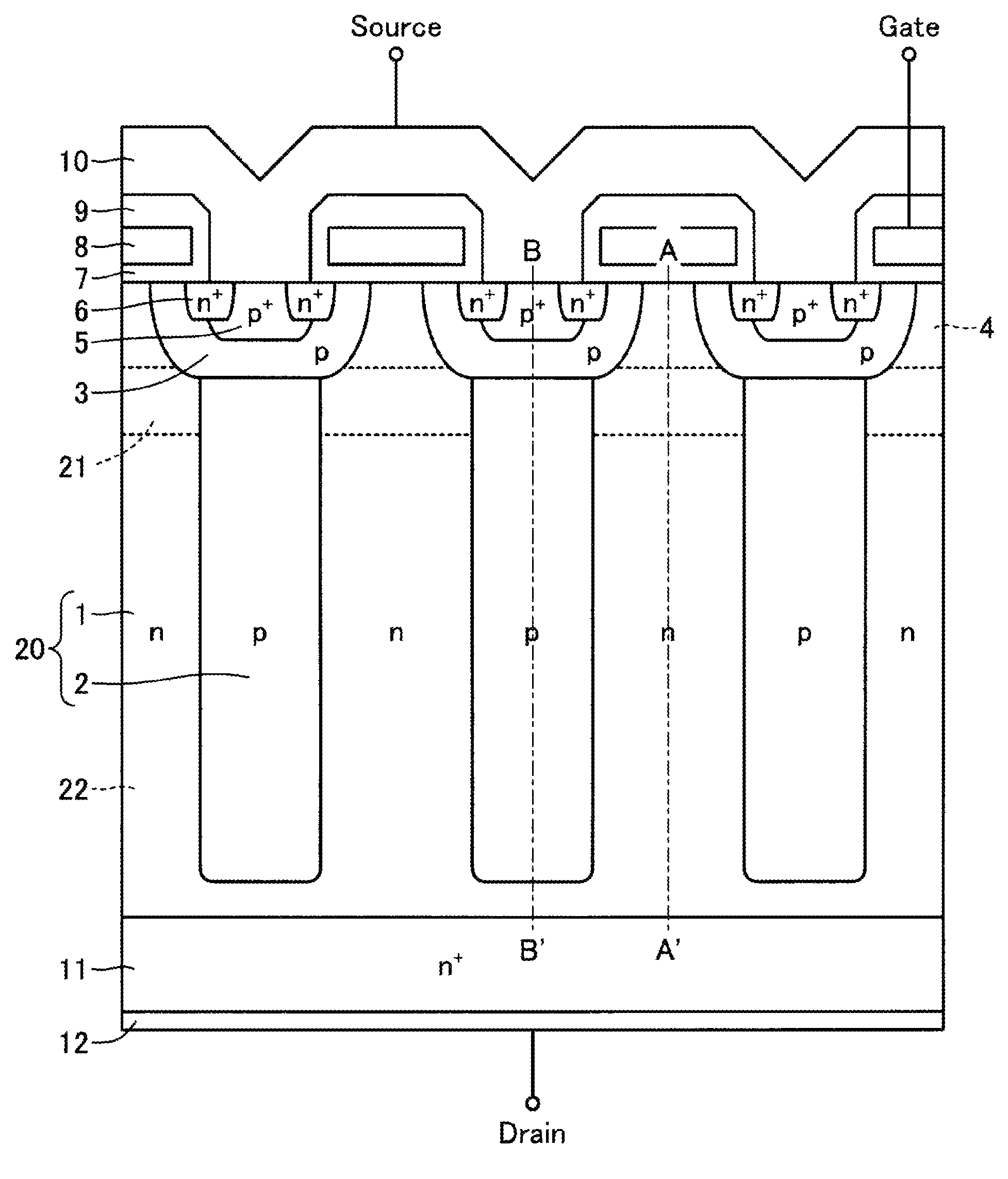
[0091]FIG. 1 is a sectional view showing a semiconductor device according to Embodiment 1. The semiconductor device, shown in FIG. 1 has an active portion on a first main surface side, and has an n+ drain region (a low resistance layer) 11 on a second main surface side. A p-base region (a second conductivity type base region) 3, an n-type surface region (a first conductivity type surface region) 4, a p+ contact region 5, an n+ source region 6, a gate insulating film 7, a gate electrode 8, an interlayer insulating film 9, and a source electrode 10 are provided as, for example, a planar type MOSFET surface structure in the active portion. A drain electrode 12 in contact with the n+ drain region 11 is provided on the second main surface.

[0092]A parallel p-n layer 20 is provided as a drift layer between the active portion and the n+ drain region 11. The parallel p-n layer 20 is formed by an n-type region (a first conductivity type region) 1 and a p-type region (a second conductivity typ...

embodiment 2

[0103]FIG. 3 is a sectional view showing a semiconductor device according to Embodiment 2. A trench structure may also be applied in Embodiment 1.

[0104]In Embodiment 2, a trench structure, wherein a gate electrode 18 is provided across a gate insulating film 17 inside a trench, is configured on the upper end side of the n-type region 1. The p-base region 3 and source region 6 are in contact with the gate insulating film 17 provided on a trench side wall. The source electrode 10 is isolated from the gate electrode 18 by an interlayer insulating film 19. No n-type surface region is provided.

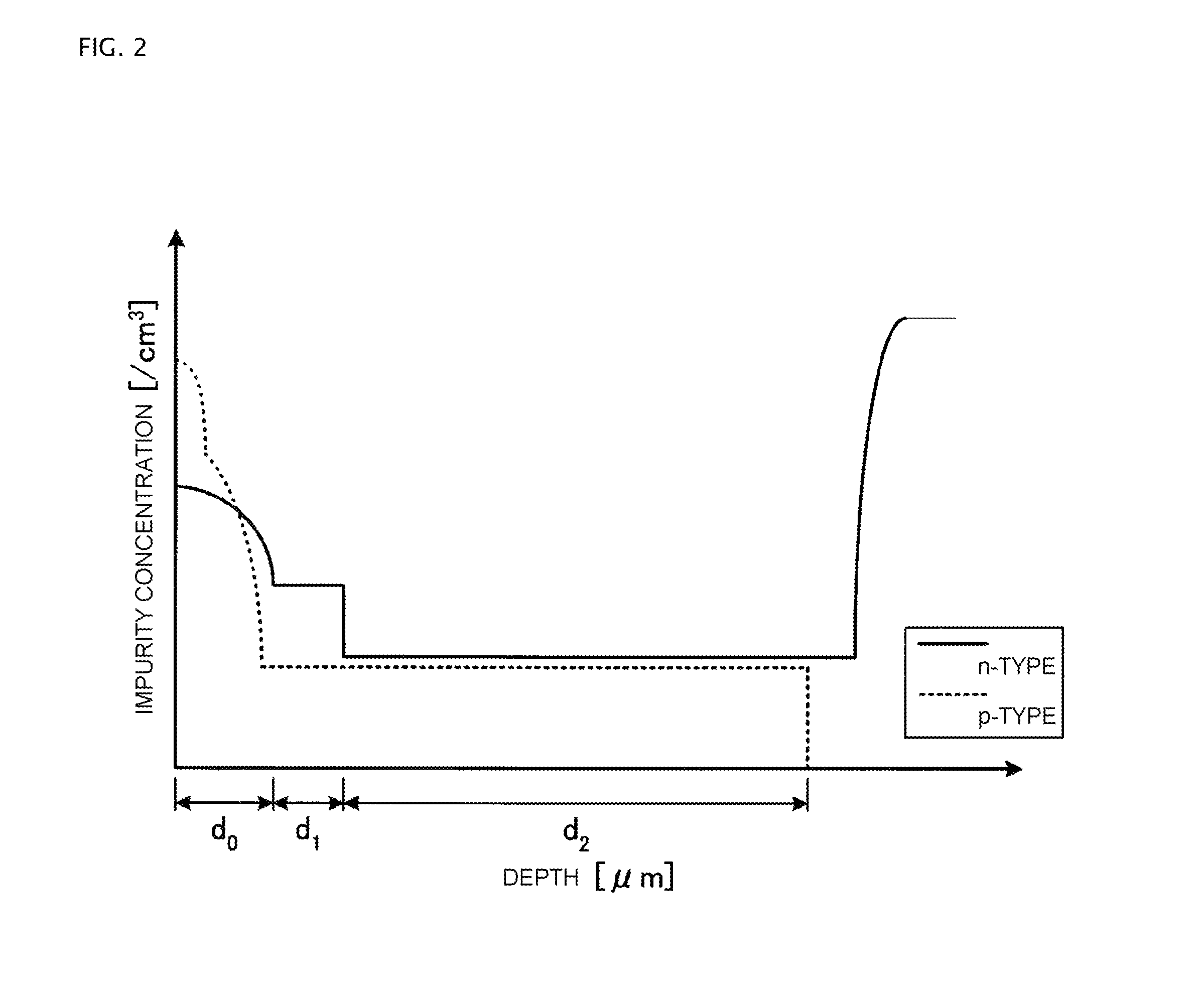
[0105]An n-type impurity concentration distribution of the n-type region 1 along the cut line of C-C′ in FIG. 3 is the same as the n-type impurity concentration distribution of the n-type region 1 along the cut line of A-A′ in Embodiment 1 (refer to FIG. 1 and FIG. 2). As no n-type surface region is provided in the semiconductor device shown in FIG. 3, the n-type impurity concentration distribution...

embodiment 3

[0107]FIG. 4 is a sectional view showing a semiconductor device according to Embodiment 3. In FIG. 4, only one p-n junction of the parallel p-n layer 20 is shown (hereafter, the same also applies in FIG. 6 and FIG. 8). In Embodiment 1, the impurity concentration of the first main surface side of the p-type region 2 may be higher than the impurity concentration of the second main surface side of the p-type region 2.

[0108]In Embodiment 3, a p-type high concentration region (a second conductivity type high concentration region) 23 is provided on the first main surface side of the p-type region 2. The p-type high concentration region 23 is in contact with the lower end of the p-base region 3. Also, the p-type high concentration region 23 has a higher impurity concentration than a region (hereafter referred to as a p-type low concentration region) 24 of the p-type region 2 excepting the p-type high concentration region 23.

[0109]Also, the p-type high concentration region 23 has the same t...


PUM


Abstract

A parallel p-n layer (20) is provided as a drift layer between an active portion and an n+ drain region (11). The parallel p-n layer (20) is formed by an n-type region (1) and a p-type region (2) being repeatedly alternately joined. An n-type high concentration region (21) is provided on a first main surface side of the n-type region (1). The n-type high concentration region (21) has an impurity concentration higher than that of an n-type low concentration region (22) provided on a second main surface side of the n-type region (1). The n-type high concentration region (21) has an impurity concentration 1.2 times or more, 3 times or less, preferably 1.5 times or more, 2.5 times or less, greater than that of the n-type low concentration region (22). Also, the n-type high concentration region (21) has one-third or less, preferably one-eighth or more, one-fourth or less, of the thickness of a region of the n-type region (1) adjacent to the p-type region (2).

Description

[0001]This application is a U.S. National Phase Application of PCT International Application PCT / JP2011 / 051831 filed on Jan. 28, 2011, which is based on and claims priority from JP 2010-017901 filed on Jan. 29, 2010, the contents of which is incorporated herein in its entirety by reference.TECHNICAL FIELD[0002]The present invention relates to a semiconductor device.BACKGROUND ART[0003]In general, semiconductor devices are classified into lateral semiconductor devices, wherein electrodes are formed on one surface of a semiconductor substrate, and vertical semiconductor devices, which have electrodes on both surfaces of a semiconductor substrate. In the vertical semiconductor device, a direction in which a drift current flows in an on-state, and a direction in which a depletion layer caused by a reverse bias voltage extends in an off-state, are the same. In a conventional planar n-channel vertical MOSFET (MOSFET: metal oxide semiconductor field effect transistor), a high resistivity n...

Claims


Application Information

Patent Timeline
IPC IPC(8): H01L29/66H01L29/78H01L29/06H01L29/08H01L29/10
CPCH01L29/7802H01L29/0634H01L29/0878H01L29/66712H01L29/7813H01L29/1095
Inventor ONISHIKITAMURA, MUTSUMISUGI, AKIOTAKEI, MANABU
Owner FUJI ELECTRIC CO LTD
Why Eureka
Try Eureka