Micro-light-emitting diode

a light-emitting diode and micro-led technology, applied in the direction of basic electric elements, electrical apparatus, semiconductor devices, etc., can solve the problems of reducing the light emission reducing the efficiency of the led, and a large number of surface and defect states, so as to increase the efficiency of the micro-led and reduce the effect of non-radiative recombination occurring at the side surface of the micro-led

Active Publication Date: 2015-08-11
MIKRO MESA TECH
View PDF3 Cites 70 Cited by
  • Summary
  • Abstract
  • Description
  • Claims
  • Application Information

AI Technical Summary

Benefits of technology

[0010]The opening defines the contact interface between the first electrode and the second type semiconductor layer. When the micro-LED is forward biased, charge carriers flow from the contact interface between the first electrode and the second type semiconductor layer to the junction of the first type semiconductor layer and the second type semiconductor layer. Since the first shortest distance is greater than or equal to 1 μm, charge carriers spreading to the side surface of the micro-LED are rare or none. Therefore, the non-radiative recombination occurring at the side surface of the micro-LED can be reduced, thereby increasing the efficiency of the micro-LED.
[0011]Furthermore, since the opening limits the area where the current goes into the micro-LED, the current density within the emitting area of the micro-LED increases and can be more uniform, thereby increasing the efficiency of the micro-LED.
[0012]Moreover, since charge carriers spreading to the side surface of the micro-LED are rare or none, the leakage currents of the micro-LED can be reduced regardless of the lattice defects in the side surface of the micro-LED.
[0013]Furthermore, since the opening makes the emitting area of the micro-LED smaller than the size of the micro-LED, it is possible to continue miniaturization of the emitting area of the micro-LED while remain the size of the micro-LED to allow the micro-LED to be manufactured with acceptable yield rate. In addition, the micro-LED with a larger size has a considerably lower electrostatic sensitivity, a considerably lower surface leakage current, and a considerably lower side surface leakage current due to the lattice defects.

Problems solved by technology

However, when electrons and holes recombine through intermediate electronic states in the semiconductor gap, then the recombination energy is emitted in the form of heat instead of photons, reducing the light emission efficiency of the LED.
On the side surface of an LED, typically there are a large number of surface and defect states.
This non-radiative recombination generates heat instead of light, considerably reducing the efficiency of the LED.
This problem becomes more and more serious as miniaturization of LEDs proceeds to microscale since electrons and holes can spread to the side surface easily in a micro-LED.
Furthermore, since electrons and holes can spread to the side surface easily in a micro-LED, the current density may be too low and uneven within the emitting area of the micro-LED.
The low and uneven current density within the emitting area of the micro-LED reduces the efficiency of the micro-LED as well.
Moreover, typically there are a large number of lattice defects in the side surface of an LED due to the etching and / or scribing process.
These lattice defects result in leakage currents.
As miniaturization of LEDs proceeds to microscale, the ratio of the lattice defects to the lattice sites of a micro-LED increases, thereby raising the ratio of the leakage currents to the total currents of the micro-LED and reducing the efficiency of the micro-LED.
In addition, transferring, controlling, operating, and handling of micro-LEDs also become more and more difficult.

Method used


Image

  • Micro-light-emitting diode
  • Micro-light-emitting diode
  • Micro-light-emitting diode

Examples


first embodiment

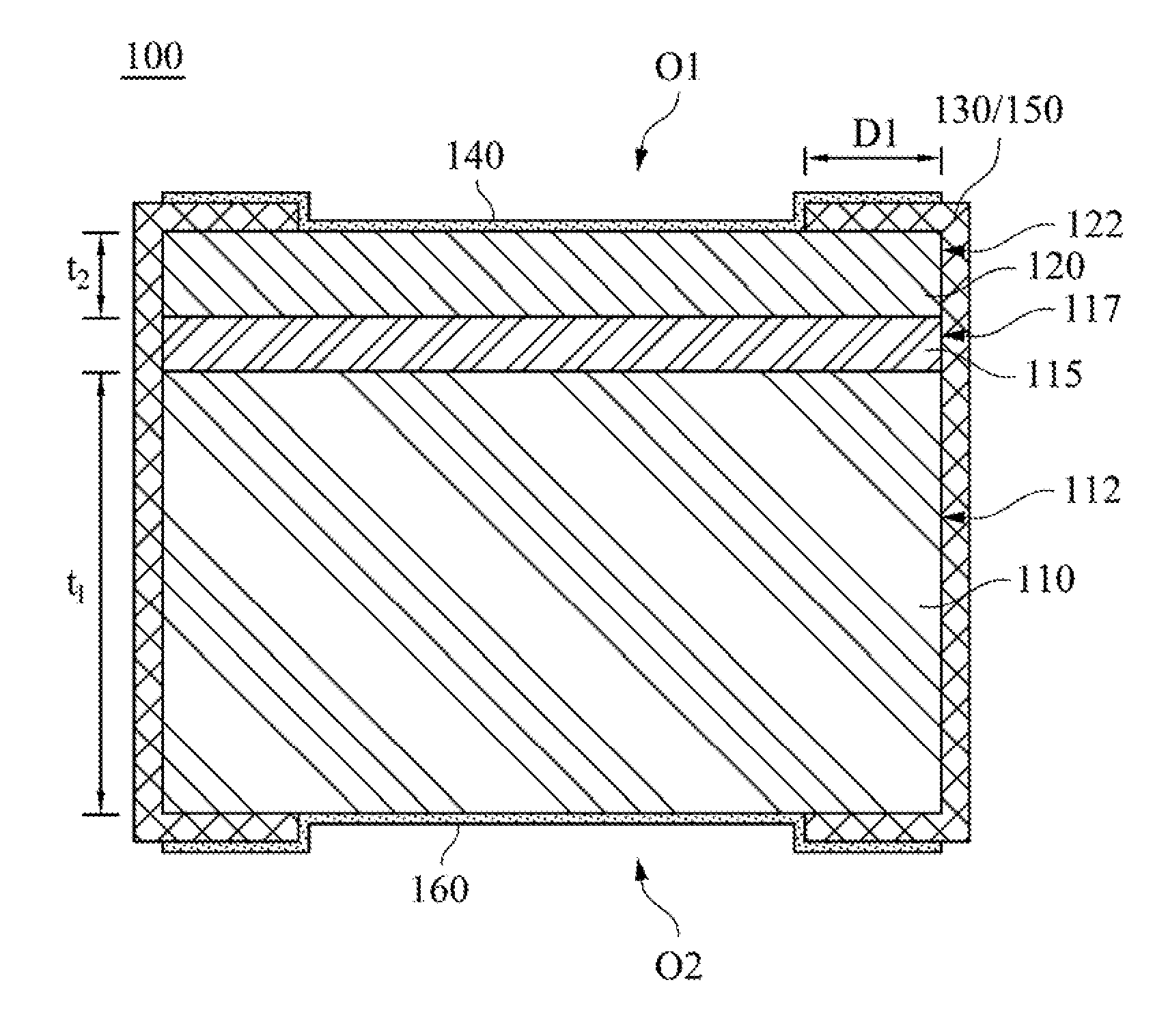
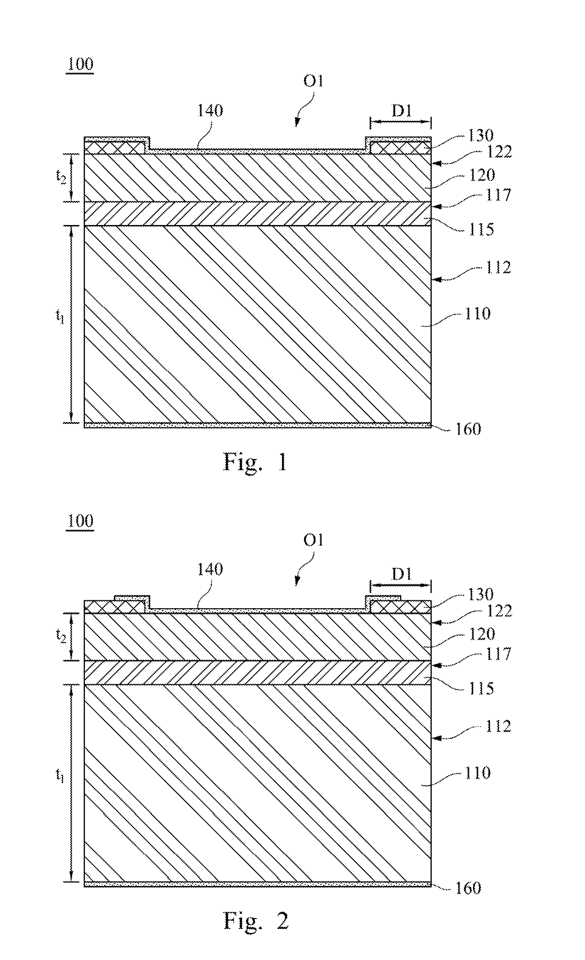
[0027]FIG. 1 is a cross-sectional view of a micro-light-emitting diode (micro-LED) 100 according to this invention. The micro-LED 100 includes a first type semiconductor layer 110, an active layer 115, a second type semiconductor layer 120, a first dielectric layer 130, and a first electrode 140. The second type semiconductor layer 120 is disposed above the first type semiconductor layer 110. The active layer 115 is disposed between the first type semiconductor layer 110 and the second type semiconductor layer 120. The first dielectric layer 130 is disposed on the second type semiconductor layer 120. The first dielectric layer 130 has at least one opening O1 therein to expose at least one part of the second type semiconductor layer 120. A first shortest distance D1 between an edge of the opening O1 and a side surface 122 of the second type semiconductor layer 120 is greater than or equal to 1 μm. The first electrode 140 is partially disposed on the first dielectric layer 130 and is ...

third embodiment

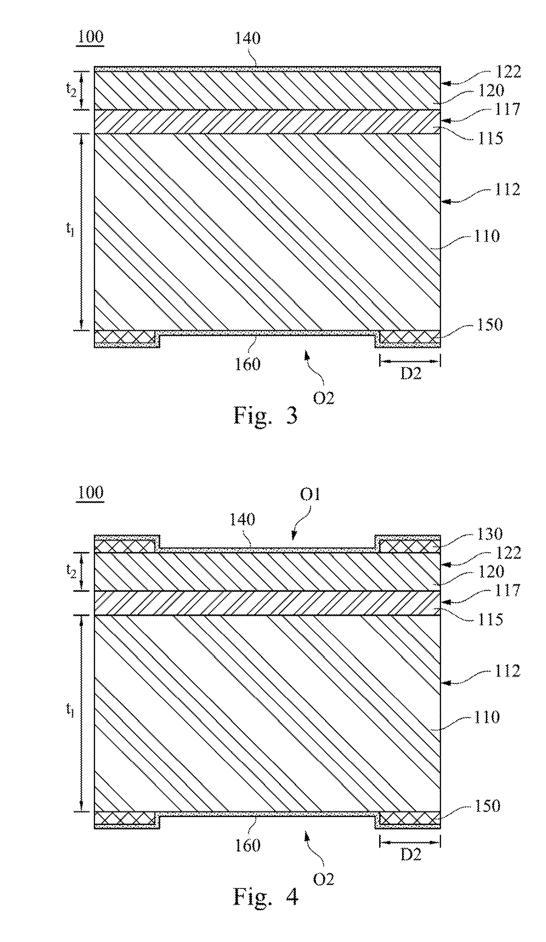
[0056]FIG. 4 is a cross-sectional view of a micro-LED 100 according to the forth embodiment of this invention. The difference between this embodiment and the first or third embodiment is that the micro-LED 100 of FIG. 4 includes both the first dielectric layer 130 with the opening O1 and the second′ dielectric layer 150 with the opening O2.

[0057]Other details regarding the micro-LED 100 of FIG. 4 are similar to the micro-LEDs 100 of FIGS. 1 and 3 and therefore are not repeated here to avoid duplicity.

fifth embodiment

[0058]FIG. 5 is a cross-sectional view of a micro-LED 100 according to this invention. Similar to the first dielectric layer 130 of FIG. 1, the first dielectric layer 130 of FIG. 5 partially cover a major surface of the second type semiconductor layer 120 distal to the first type semiconductor layer 110. The difference between the first dielectric layer 130 of FIG. 5 and the first dielectric layer 130 of FIG. 1 is that the first dielectric layer 130 of FIG. 5 further at least partially covers the side surface 122. In this configuration, the side surface 122 can be protected from moisture and mechanical damage by the first dielectric layer 130.

[0059]Other details regarding the micro-LED 100 of FIG. 5 are similar to the micro-LED 100 of FIG. 1 and therefore are not repeated here to avoid duplicity.


PUM


Abstract

A micro-light-emitting diode (micro-LED) includes a first type semiconductor layer, a second type semiconductor, a first dielectric layer, and a first electrode. The second type semiconductor layer is disposed on or above the first type semiconductor layer. The first dielectric layer is disposed on the second type semiconductor layer. The first dielectric layer has at least one opening therein to expose at least one part of the second type semiconductor layer. A first shortest distance between an edge of the opening of the first dielectric layer and a side surface of the second type semiconductor layer is greater than or equal to 1 μm. The first electrode is partially disposed on the first dielectric layer and is electrically coupled with the exposed part of the second type semiconductor layer through the opening of the first dielectric layer.

Description

BACKGROUND[0001]1. Technical Field[0002]The present disclosure relates to micro-light-emitting diodes (micro-LEDs).[0003]2. Description of Related Art[0004]In the recent years, light-emitting diodes (LEDs) have become popular in general and commercial lighting applications. As light sources, LEDs have many advantages including lower energy consumption, longer lifetime, smaller size, and faster switching, and hence conventional lighting, such as incandescent lighting, is gradually replaced by LED lights.[0005]In an LED, when electrons and holes recombine across the semiconductor gap, the recombination energy is emitted in the form of photons and generates light. This recombination mechanism is the so-called radiative recombination. However, when electrons and holes recombine through intermediate electronic states in the semiconductor gap, then the recombination energy is emitted in the form of heat instead of photons, reducing the light emission efficiency of the LED. This recombinat...

Claims


Application Information

Patent Timeline
Patent Type & Authority Patents(United States)
IPC IPC(8): H01L33/38H01L33/44H01L33/20
CPCH01L33/38H01L33/44H01L33/20H01L33/02
Inventor CHANG, PEI-YU
Owner MIKRO MESA TECH
Why Eureka
Try Eureka